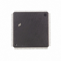
DP83905AVQB National Semiconductor, DP83905AVQB Datasheet - Page 79

DP83905AVQB
Manufacturer Part Number
DP83905AVQB
Description
IC CONTROLR AT/LAN TP IN 160PQFP
Manufacturer
National Semiconductor
Series
AT/LANTIC™r
Datasheet
1.DP83905AVQB.pdf
(80 pages)
Specifications of DP83905AVQB
Controller Type
AT, LAN Twisted-Pair Interface Controller
Voltage - Supply
4.75 V ~ 5.25 V
Current - Supply
100mA
Operating Temperature
0°C ~ 70°C
Mounting Type
Surface Mount
Package / Case
160-BFQFP
Lead Free Status / RoHS Status
Contains lead / RoHS non-compliant
Interface
-
Other names
*DP83905AVQB
Available stocks
Company
Part Number
Manufacturer
Quantity
Price
Company:
Part Number:
DP83905AVQB
Manufacturer:
Texas Instruments
Quantity:
10 000
Part Number:
DP83905AVQB
Manufacturer:
NS/国半
Quantity:
20 000
9 0 AC Timing Test Conditions
Input Pulse Levels (TTL CMOS)
Input Rise and Fall Times (TTL CMOS)
Input and Output Reference Levels
Input Pulse Levels (Diff )
Input and Output
Reference Levels (Diff )
TRI-STATE Reference Levels
Output Load (See Figure Below)
All specifications are valid only if the mandatory isolation is
employed and all differential signals are taken to be at the
AUI side of the pulse transformer
Output Load (See Figure Below)
Note 1 Load Capacitance used depends on output type (includes scope
and jig capacitance)
Note 2 Specifications which measure delays from an active state to a high
impedance state are not guaranteed by production test but are character-
ized using 70 pF and are correlated to determine true driver turn-off time by
eliminating inherent R-C delay times in measurements
Note 3 S1
Note 4 Pull-up load for CHRDY
(TTL CMOS)
For 3SL MOS TPI AUI C
For 3SH OCH C
S1
S1
S1
e
e
e
e
e
active low to High Impedance measurements
active high to High Impedance measurements
Open for timing test for push pull outputs
V
GND for V
V
GND for High Impedance to active high and
CC
CC
for V
for High Impedance to active low and
L
e
OL
OH
IO16
240 pF
M16
test
test
L
e
e
e
e
1 k
300
300
50 pF
b
350 mV to
Float ( V)
the Differential
50% Point of
GND to 3 0V
TL F 11498– 61
b
1315 mV
g
1 3V
0 5V
5 ns
79
Pin Capacitance
DERATING FACTOR
Output timing is measured with a purely capacitive load of
50 pF or 240 pF The following correction factor can be
used for other loads (Note This factor is preliminary)
Derating for 3SL MOS
Derating for 3SH OCL TPI
Note In the above diagram the TX
AUI side of the isolation (pulse transformer) The pulse transformer used for
all testing is a 100 H
Symbol
C
C
IN
OUT
Input Capacitance
Output Capacitance
AUI Transmit Test Load
g
0 1% Pulse Engineering PE64103
Parameter
e
E 0 05 ns pF
T
a
e
A
and TX
e
E 0 03 ns pF
25 C f
b
signals are taken from the
e
Typ
10
7
1 MHz
TL F 11498 – 62
Units
pF
pF


