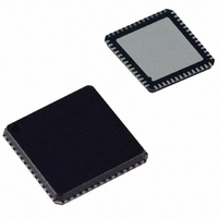
AD9959BCPZ Analog Devices Inc, AD9959BCPZ Datasheet - Page 20

AD9959BCPZ
Manufacturer Part Number
AD9959BCPZ
Description
IC DDS QUAD 10BIT DAC 56LFCSP
Manufacturer
Analog Devices Inc
Datasheet
1.AD9959BCPZ.pdf
(44 pages)
Specifications of AD9959BCPZ
Resolution (bits)
10 b
Design Resources
Phase Coherent FSK Modulator (CN0186)
Master Fclk
500MHz
Tuning Word Width (bits)
32 b
Voltage - Supply
1.71 V ~ 1.96 V
Operating Temperature
-40°C ~ 85°C
Mounting Type
Surface Mount
Package / Case
56-LFCSP
Sampling Rate
500MSPS
Input Channel Type
Serial
Supply Voltage Range - Analog
1.71V To 1.89V
Supply Current
160mA
Digital Ic Case Style
CSP
Data Interface
Serial, SPI
Lead Free Status / RoHS Status
Lead free / RoHS Compliant
Lead Free Status / RoHS Status
Lead free / RoHS Compliant, Lead free / RoHS Compliant
Available stocks
Company
Part Number
Manufacturer
Quantity
Price
Company:
Part Number:
AD9959BCPZ
Manufacturer:
ADI
Quantity:
1 648
Part Number:
AD9959BCPZ
Manufacturer:
ADI/亚德诺
Quantity:
20 000
AD9959
Single-Tone Mode—Matched Pipeline Delay
In single-tone mode, the AD9959 offers matched pipeline delay
to the DAC input for all frequency, phase, and amplitude changes.
This avoids having to deal with different pipeline delays between
the three input ports for such applications. The feature is enabled
by asserting the matched pipe delays active bit found in the
channel function register (CFR, Register 0x03). This feature
is available in single-tone mode only.
REFERENCE CLOCK MODES
The AD9959 supports multiple reference clock configurations
to generate the internal system clock. As an alternative to
clocking the part directly with a high frequency clock source,
the system clock can be generated using the internal, PLL-based
reference clock multiplier. An on-chip oscillator circuit is also
available for providing a low frequency reference signal by
connecting a crystal to the clock input pins. Enabling these
features allows the part to operate with a low frequency clock
source and still provide a high update rate for the DDS and
DAC. However, using the clock multiplier changes the output
phase noise characteristics. For best phase noise performance,
a clean, stable clock with a high slew is required (see Figure 17
and Figure 18).
Enabling the PLL allows multiplication of the reference clock
frequency from 4× to 20×, in integer steps. The PLL multiplica-
tion value is represented by a 5-bit multiplier value. These bits
are located in Function Register 1 (FR1, Register 0x01), Bits[22:18]
(see the Register Maps and Bit Descriptions section).
When FR1[22:18] is programmed with values ranging from
4 to 20 (decimal), the clock multiplier is enabled. The integer
value in the register represents the multiplication factor. The
system clock rate with the clock multiplier enabled is equal to
the reference clock rate multiplied by the multiplication factor.
If FR1[22:18] is programmed with a value less than 4 or greater
than 20, the clock multiplier is disabled and the multiplication
factor is effectively 1.
Whenever the PLL clock multiplier is enabled or the multiplica-
tion value is changed, time should be allowed to lock the PLL
(typically 1 ms).
Note that the output frequency of the PLL is restricted to a
frequency range of 100 MHz to 500 MHz. However, there is a
VCO gain control bit that must be used appropriately. The VCO
gain control bit defines two ranges (low/high) of frequency
output. The VCO gain control bit defaults to low (see Table 1
for details).
Table 4. Clock Configuration
CLK_MODE_SEL, Pin 24
High = 1.8 V Logic
High = 1.8 V Logic
Low
Low
FR1[22:18] PLL Divider Ratio = M
4 ≤ M ≤ 20
M < 4 or M > 20
4 ≤ M ≤ 20
M < 4 or M > 20
Crystal Oscillator Enabled
Yes
Yes
No
No
Rev. B | Page 20 of 44
The charge pump current in the PLL defaults to 75 μA. This
setting typically produces the best phase noise characteristics.
Increasing the charge pump current may degrade phase noise,
but it decreases the lock time and changes the loop bandwidth.
Enabling the on-chip oscillator for crystal operation is performed
by driving CLK_MODE_SEL (Pin 24) to logic high (1.8 V
logic). With the on-chip oscillator enabled, connection of an
external crystal to the REF_CLK and REF_CLK inputs is made,
producing a low frequency reference clock. The frequency of
the crystal must be in the range of 20 MHz to 30 MHz.
Table 4 summarizes the clock modes of operation. See Table 1
for more details.
Reference Clock Input Circuitry
The reference clock input circuitry has two modes of operation
controlled by the logic state of Pin 24 (CLK_MODE_SEL). The
first mode (logic low) configures as an input buffer. In this
mode, the reference clock must be ac-coupled to the input due
to internal dc biasing. This mode supports either differential
or single-ended configurations. If single-ended mode is chosen,
the complementary reference clock input (Pin 22) should be
decoupled to AVDD or AGND via a 0.1 μF capacitor. Figure 33
to Figure 35 exemplify typical reference clock configurations for
the AD9959.
The reference clock inputs can also support an LVPECL or
PECL driver as the reference clock source.
The second mode of operation (Pin 24 = logic high = 1.8 V)
provides an internal oscillator for crystal operation. In this
mode, both clock inputs are dc-coupled via the crystal leads
and are bypassed. The range of crystal frequencies supported is
from 20 MHz to 30 MHz. Figure 35 shows the configuration
for using a crystal.
LVPECL/
Figure 33. Differential Coupling from Single-Ended Source
DRIVER
PECL
SOURCE
REFCLK
Figure 34. Differential Clock Source Hook-Up
f
f
f
f
System Clock (f
SYSCLK
SYSCLK
SYSCLK
SYSCLK
= f
= f
= f
= f
TERMINATION
OSC
OSC
REFCLK
REFCLK
× M
BALUN
× M
1:1
SYSCLK
)
50Ω
Min/Max Freq. Range (MHz)
100 < f
20 < f
100 < f
0 < f
0.1µF
0.1µF
0.1µF
0.1µF
SYSCLK
SYSCLK
SYSCLK
SYSCLK
REF_CLK
REF_CLK
< 500
PIN 23
PIN 22
< 30
< 500
< 500
REF_CLK
REF_CLK
PIN 23
PIN 22


