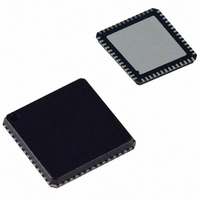
AD9959BCPZ Analog Devices Inc, AD9959BCPZ Datasheet - Page 33

AD9959BCPZ
Manufacturer Part Number
AD9959BCPZ
Description
IC DDS QUAD 10BIT DAC 56LFCSP
Manufacturer
Analog Devices Inc
Datasheet
1.AD9959BCPZ.pdf
(44 pages)
Specifications of AD9959BCPZ
Resolution (bits)
10 b
Design Resources
Phase Coherent FSK Modulator (CN0186)
Master Fclk
500MHz
Tuning Word Width (bits)
32 b
Voltage - Supply
1.71 V ~ 1.96 V
Operating Temperature
-40°C ~ 85°C
Mounting Type
Surface Mount
Package / Case
56-LFCSP
Sampling Rate
500MSPS
Input Channel Type
Serial
Supply Voltage Range - Analog
1.71V To 1.89V
Supply Current
160mA
Digital Ic Case Style
CSP
Data Interface
Serial, SPI
Lead Free Status / RoHS Status
Lead free / RoHS Compliant
Lead Free Status / RoHS Status
Lead free / RoHS Compliant, Lead free / RoHS Compliant
Available stocks
Company
Part Number
Manufacturer
Quantity
Price
Company:
Part Number:
AD9959BCPZ
Manufacturer:
ADI
Quantity:
1 648
Part Number:
AD9959BCPZ
Manufacturer:
ADI/亚德诺
Quantity:
20 000
SERIAL I/O MODES OF OPERATION
The following are the four programmable modes of serial I/O
port operation:
•
•
•
•
Table 26 displays the function of all six serial I/O interface pins,
depending on the mode of serial I/O operation programmed.
Table 26. Serial I/O Port Pin Function vs. Serial I/O Mode
Pin
SCLK
CS
SDIO_0
SDIO_1
SDIO_2
SDIO_3
1
The two bits in the channel select register, CSR[2:1], set the
serial I/O mode of operation and are defined in Table 27.
Table 27. Serial I/O Mode of Operation
Serial I/O Mode Select
(CSR[2:1])
00
01
10
11
Single-Bit Serial (2-Wire and 3-Wire) Modes
The single-bit serial mode interface allows read/write access to
all registers that configure the AD9959. MSB first or LSB first
transfer formats are supported. In addition, the single-bit serial
mode interface port can be configured either as a single pin I/O,
which allows a 2-wire interface, or as two unidirectional pins
for input/output, which enable a 3-wire interface. Single-bit
mode allows the use of the SYNC_I/O function.
In serial mode, these pins (SDIO_0/SDIO_1/SDIO_2/SDIO_3) can be used for
RU/RD operation
Single-bit serial 2-wire mode (default mode)
Single-bit serial 3-wire mode
2-bit serial mode
4-bit serial mode (SYNC_I/O not available)
Single-Bit
Serial 2-Wire
Mode
Serial clock
Chip select
Serial data I/O
Not used for
SDIO
Not used for
SDIO
SYNC_I/O
1
1
.
Single-Bit
Serial 3-Wire
Mode
Serial clock
Chip select
Serial data in
Not used for
SDIO
Serial data
out (SDO)
SYNC_I/O
Mode of Operation
Single-bit serial mode (2-wire mode)
Single-bit serial mode (3-wire mode)
2-bit serial mode
4-bit serial mode
1
Serial clock
2-Bit
Serial
Mode
Chip select
Serial data
I/O
Serial data
I/O
Not used
for SDIO
SYNC_I/O
1
4-Bit
Serial
Mode
Serial
clock
Chip
select
Serial
data I/O
Serial
data I/O
Serial
data I/O
Serial
data I/O
Rev. B | Page 33 of 44
In single-bit serial mode, 2-wire interface operation, the
SDIO_0 pin is the single serial data I/O pin. In single-bit serial
mode 3-wire interface operation, the SDIO_0 pin is the serial
data input pin and the SDIO_2 pin is the output data pin.
Regardless of the number of wires used in the interface, the
SDIO_3 pin is configured as an input and operates as the
SYNC_I/O pin in the single-bit serial mode and 2-bit serial
mode. The SDIO_1 pin is unused in this mode (see Table 26).
2-Bit Serial Mode
The SPI port operation in 2-bit serial mode is identical to the
SPI port operation in single-bit serial mode, except that two bits
of data are registered on each rising edge of SCLK. Therefore, it
only takes four clock cycles to transfer eight bits of information.
The SDIO_0 pin contains the even numbered data bits using
the notation D[7:0], and the SDIO_1 pin contains the odd
numbered data bits. This even and odd numbered pin/data
alignment is valid in both MSB and LSB first formats (see
Figure 44).
4-Bit Serial Mode
The SPI port in 4-bit serial mode is identical to the SPI port in
single-bit serial mode, except that four bits of data are registered
on each rising edge of SCLK. Therefore, it takes only two clock
cycles to transfer eight bits of information. The SDIO_0 and
SDIO_2 pins contain even numbered data bits using the notation
D[7:0], and the SDIO_0 pin contains the LSB of the nibble. The
SDIO_1 and SDIO_3 pins contain the odd numbered data bits,
and the SDIO_1 pin contains the LSB of the nibble to be accessed.
Note that when programming the device for 4-bit serial mode,
it is important to keep the SDIO_3 pin at Logic 0 until the device is
programmed out of the single-bit serial mode. Failure to do so
can result in the serial I/O port controller being out of sequence.
Figure 43 through Figure 45 represent write timing diagrams
for each of the serial I/O modes available. Both MSB and LSB
first modes are shown. LSB first bits are shown in parentheses.
The clock stall low/high feature shown is not required. It is used
to show that data (SDIO) must have the proper setup time
relative to the rising edge of SCLK.
Figure 46 through Figure 49 represent read timing diagrams for
each of the serial I/O modes available. Both MSB and LSB first
modes are shown. LSB first bits are shown in parentheses. The
clock stall low/high feature shown is not required. It is used to
show that data (SDIO) must have the proper setup time relative
to the rising edge of SCLK for the instruction byte and the read
data that follows the falling edge of SCLK.
AD9959


