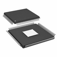
AD9910BSVZ Analog Devices Inc, AD9910BSVZ Datasheet - Page 36

AD9910BSVZ
Manufacturer Part Number
AD9910BSVZ
Description
IC DDS 1GSPS 14BIT PAR 100TQFP
Manufacturer
Analog Devices Inc
Datasheet
1.AD9910BSVZ-REEL.pdf
(64 pages)
Specifications of AD9910BSVZ
Design Resources
Synchronizing Multiple AD9910 1 GSPS Direct Digital Synthesizers (CN0121)
Resolution (bits)
14 b
Master Fclk
1GHz
Tuning Word Width (bits)
32 b
Voltage - Supply
1.8V, 3.3V
Operating Temperature
-40°C ~ 85°C
Mounting Type
Surface Mount
Package / Case
100-TQFP Exposed Pad, 100-eTQFP, 100-HTQFP, 100-VQFP
Pll Type
Frequency Synthesis
Frequency
1GHz
Supply Current
29mA
Supply Voltage Range
1.71V To 1.89V
Digital Ic Case Style
TQFP
No. Of Pins
100
Operating Temperature Range
-40°C To +85°C
Lead Free Status / RoHS Status
Lead free / RoHS Compliant
For Use With
AD9910/PCBZ - BOARD EVAL FOR AD9910 1GSPS
Lead Free Status / RoHS Status
Lead free / RoHS Compliant, Lead free / RoHS Compliant
Available stocks
Company
Part Number
Manufacturer
Quantity
Price
Company:
Part Number:
AD9910BSVZ
Manufacturer:
AVAGO
Quantity:
1 400
Company:
Part Number:
AD9910BSVZ
Manufacturer:
ADI
Quantity:
509
Company:
Part Number:
AD9910BSVZ
Manufacturer:
Analog Devices Inc
Quantity:
10 000
Part Number:
AD9910BSVZ
Manufacturer:
ADI/亚德诺
Quantity:
20 000
Company:
Part Number:
AD9910BSVZ-REEL
Manufacturer:
Analog Devices Inc
Quantity:
10 000
AD9910
RAM Ramp-Up Internal Profile Control Mode
Table 14. RAM Internal Profile Control Modes
Internal Profile Control Bits (CFR1[20:17])
0000
0001
0010
0011
0100
0101
0110
0111
1000
1001
1010
1011
1100
1101
1110
1111
Ramp up internal profile control mode is invoked via the four
internal profile control bits (rather than through the RAM
profile mode control bits in the RAM profile registers).
If any of the internal profile control bits is set, then the RAM
profile mode control bits of the RAM profile registers are
ignored. The no-dwell high bit is ignored in this mode. The
internal profile control mode is identical to ramp-up mode
except that profile switching is done automatically and
internally; the state of the PROFILE[2:0] pins is ignored.
Profiles cycle according to Table 14.
There are two types of waveform generation types available
under internal profile control: burst waveforms and continuous
waveforms. With both types, the state machine begins with the
waveform specified by the waveform start address, waveform
end address, and address ramp rate in Profile 0. After reaching
the waveform end address of Profile 0, the state machine automati-
cally advances to the next profile and initiates the specified
waveform as defined by the new profile parameters. After the
state machine reaches the waveform end address of the new
profile, it advances to the next profile. This action continues
until the state machine reaches the waveform end address of
the last profile, as governed by the internal profile control bits in
Control Function Register 1 (CFR1) per Table 14.
Waveform Type
Burst
Burst
Burst
Burst
Burst
Burst
Burst
Continuous
Continuous
Continuous
Continuous
Continuous
Continuous
Continuous
Rev. C | Page 36 of 64
At this point, the next course of action depends on whether the
waveform type is burst or continuous. For burst waveforms, the
state machine halts operation after reaching the waveform end
address of the final profile. For continuous waveforms, the state
machine automatically jumps to Profile 0 and continues the
automatic waveform generation by sequentially advancing
through the profiles. This process continues indefinitely until
the internal profile control bits are reprogrammed and an I/O
update is asserted.
A burst waveform timing diagram is exemplified in Figure 44.
The diagram assumes that the internal profile control bits in
Register CFR1 are programmed as 0010, the start address in
RAM Profile 1 is greater than the end address in RAM Profile 0,
and that the start address in RAM Profile 2 is greater than the
end address in RAM Profile 1. However, the block of RAM
associated with each profile can be chosen arbitrarily based on
the waveform start address and waveform end address for each
profile. Furthermore, the example shows how different Δt
values associated with each profile can be used.
Internal Profile Control Description
Internal profile control disabled.
Execute Profile 0, then Profile 1, then halt.
Execute Profile 0 to Profile 2, then halt.
Execute Profile 0 to Profile 3, then halt.
Execute Profile 0 to Profile 4, then halt.
Execute Profile 0 to Profile 5, then halt.
Execute Profile 0 to Profile 6, then halt.
Execute Profile 0 to Profile 7, then halt.
Execute Profile 0, then Profile 1, continuously.
Execute Profile 0 to Profile 2, continuously.
Execute Profile 0 to Profile 3, continuously.
Execute Profile 0 to Profile 4, continuously.
Execute Profile 0 to Profile 5, continuously.
Execute Profile 0 to Profile 6, continuously.
Execute Profile 0 to Profile 7, continuously.
Invalid.


