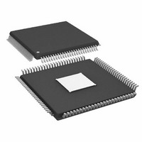
AD9910BSVZ Analog Devices Inc, AD9910BSVZ Datasheet - Page 40

AD9910BSVZ
Manufacturer Part Number
AD9910BSVZ
Description
IC DDS 1GSPS 14BIT PAR 100TQFP
Manufacturer
Analog Devices Inc
Datasheet
1.AD9910BSVZ-REEL.pdf
(64 pages)
Specifications of AD9910BSVZ
Design Resources
Synchronizing Multiple AD9910 1 GSPS Direct Digital Synthesizers (CN0121)
Resolution (bits)
14 b
Master Fclk
1GHz
Tuning Word Width (bits)
32 b
Voltage - Supply
1.8V, 3.3V
Operating Temperature
-40°C ~ 85°C
Mounting Type
Surface Mount
Package / Case
100-TQFP Exposed Pad, 100-eTQFP, 100-HTQFP, 100-VQFP
Pll Type
Frequency Synthesis
Frequency
1GHz
Supply Current
29mA
Supply Voltage Range
1.71V To 1.89V
Digital Ic Case Style
TQFP
No. Of Pins
100
Operating Temperature Range
-40°C To +85°C
Lead Free Status / RoHS Status
Lead free / RoHS Compliant
For Use With
AD9910/PCBZ - BOARD EVAL FOR AD9910 1GSPS
Lead Free Status / RoHS Status
Lead free / RoHS Compliant, Lead free / RoHS Compliant
Available stocks
Company
Part Number
Manufacturer
Quantity
Price
Company:
Part Number:
AD9910BSVZ
Manufacturer:
AVAGO
Quantity:
1 400
Company:
Part Number:
AD9910BSVZ
Manufacturer:
ADI
Quantity:
509
Company:
Part Number:
AD9910BSVZ
Manufacturer:
Analog Devices Inc
Quantity:
10 000
Part Number:
AD9910BSVZ
Manufacturer:
ADI/亚德诺
Quantity:
20 000
Company:
Part Number:
AD9910BSVZ-REEL
Manufacturer:
Analog Devices Inc
Quantity:
10 000
AD9910
A change in state of the PROFILE pins aborts the current wave-
form, and the newly selected RAM profile is used to initiate a
new waveform.
The RAM_SWP_OVR pin switches to Logic 1 when the state
machine reaches the waveform end address, then returns to
Logic 0 at the waveform start address, toggling each time one
of these addresses is reached.
A graphic representation of the continuous bidirectional ramp
mode is shown in Figure 47. The circled numbers indicate specific
events as follows:
RAM_SWP_OVER
RAM ADRESS
I/O_UPDATE
WAVEFORM END ADDRESS
1
WAVEFORM START ADDRESS
Figure 47. Continuous Bidirectional Ramp Timing Diagram
M DDS CLOCK CYCLES
1
Rev. C | Page 40 of 64
Δ
t
2
Event 1—An I/O update or profile change has activated the RAM
continuous bidirectional ramp mode. The state machine initializes
to the waveform start address. The RAM_SWP_OVR pin resets to
Logic 0. The state machine begins incrementing through the
specified address range.
Event 2—The state machine reaches the waveform end address.
The RAM_SWP_OVR pin toggles to Logic 1.
Event 3—The state machine reaches the waveform start address.
The RAM_SWP_OVR pin toggles to Logic 0.
The continuous bidirectional ramp continues indefinitely until
the mode is changed.
Δ
t
3


