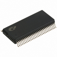
CY7C68001-56PVXC Cypress Semiconductor Corp, CY7C68001-56PVXC Datasheet - Page 5

CY7C68001-56PVXC
Manufacturer Part Number
CY7C68001-56PVXC
Description
IC USB INTERFACE SX2 56-SSOP
Manufacturer
Cypress Semiconductor Corp
Type
USBr
Series
CY7Cr
Datasheet
1.CY7C68001-56PVXC.pdf
(45 pages)
Specifications of CY7C68001-56PVXC
Package / Case
56-SSOP
Protocol
USB 2.0
Voltage - Supply
3 V ~ 3.6 V
Mounting Type
Surface Mount
Maximum Operating Temperature
+ 70 C
Minimum Operating Temperature
0 C
Mounting Style
SMD/SMT
Operating Temperature Range
0 C to + 70 C
Operating Supply Voltage
3.3 V
Core Size
8 Bit
No. Of I/o's
35
Ram Memory Size
256Byte
Embedded Interface Type
SPI, USB
Digital Ic Case Style
SSOP
Supply Voltage Range
3V To 3.6V
Rohs Compliant
Yes
Lead Free Status / RoHS Status
Lead free / RoHS Compliant
Number Of Drivers/receivers
-
Lead Free Status / Rohs Status
Lead free / RoHS Compliant
Other names
428-1864
CY7C68001-56PVXC
CY7C68001-56PVXC
Available stocks
Company
Part Number
Manufacturer
Quantity
Price
Company:
Part Number:
CY7C68001-56PVXC
Manufacturer:
CY
Quantity:
101
Company:
Part Number:
CY7C68001-56PVXC
Manufacturer:
CYPRESS
Quantity:
7
Part Number:
CY7C68001-56PVXC
Manufacturer:
CYPRESS/赛普拉斯
Quantity:
20 000
Endpoint 0 is the same for every configuration as it serves as the
CONTROL endpoint. For Endpoints 2, 4, 6, and 8, refer to
Figure 8-1.
configured by choosing either:
■
■
Some example endpoint configurations are as follows.
■
■
■
5.6.2 Default Endpoint Memory Configuration
At power-on-reset, the endpoint memories are configured as
follows:
■
■
■
■
5.7 External Interface
The SX2 presents two interfaces to the external master.
Document #: 38-08013 Rev. *J
1. A FIFO interface through which EP2, 4, 6, and 8 data flows.
2. A command interface, which is used to set up the SX2, read
One configuration from Group A and one from Group B
One configuration from Group C.
EP2: 1024 bytes double-buffered, EP6: 512 bytes
quad-buffered.
EP2: 512 bytes double-buffered, EP4: 512 bytes
double-buffered, EP6: 512 bytes double-buffered, EP8: 512
bytes double buffered.
EP2: 1024 bytes quad-buffered.
EP2: Bulk OUT, 512 bytes/packet, 2x buffered.
EP4: Bulk OUT, 512 bytes/packet, 2x buffered.
EP6: Bulk IN, 512 bytes/packet, 2x buffered.
EP8: Bulk IN, 512 bytes/packet, 2x buffered.
status, load descriptors, and access Endpoint 0.
E P 0 IN & O U T
on page 11. Endpoints 2, 4, 6, and 8 may be
E P 2
E P 4
E P 6
E P 8
G ro u p A
G ro u p B
5 1 2
5 1 2
5 1 2
5 1 2
5 1 2
5 1 2
5 1 2
5 1 2
6 4
E P 2
E P 6
Figure 5-1. Endpoint Configurations (High Speed Mode)
5 1 2
5 1 2
5 1 2
5 1 2
5 1 2
5 1 2
5 1 2
5 1 2
6 4
E P 2
E P 6
1 0 2 4
1 0 2 4
1 0 2 4
1 0 2 4
6 4
5.7.1 Architecture
The SX2 slave FIFO architecture has eight 512-byte blocks in
the endpoint RAM that directly serve as FIFO memories and are
controlled by FIFO control signals (IFCLK, CS#, SLRD, SLWR,
SLOE, PKTEND, and FIFOADR[2:0]).
The SX2 command interface is used to set up the SX2, read
status, load descriptors, and access Endpoint 0. The command
interface has its own READY signal for gating writes, and an
INT# signal to indicate that the SX2 has data to be read, or that
an interrupt event has occurred. The command interface uses
the same control signals (IFCLK, CS#, SLRD, SLWR, SLOE, and
FIFOADR[2:0]) as the FIFO interface, except for PKTEND.
5.7.2 Control Signals
FIFOADDR Lines
The SX2 has three address pins that are used to select either the
FIFOs or the command interface. The addresses correspond to
the following table.
Table 5-3. FIFO Address Lines Setting
Address/Selection FIFOADR2 FIFOADR1 FIFOADR0
E P 2
E P 6
E P 8
RESERVED
RESERVED
RESERVED
COMMAND
FIFO2
FIFO4
FIFO6
FIFO8
G ro u p C
5 1 2
5 1 2
5 1 2
5 1 2
5 1 2
5 1 2
5 1 2
5 1 2
6 4
E P 2
E P 8
0
0
0
0
1
1
1
1
1 0 2 4
1 0 2 4
1 0 2 4
5 1 2
5 1 2
6 4
E P 2
0
0
1
1
0
0
1
1
CY7C68001
1 0 2 4
1 0 2 4
1 0 2 4
1 0 2 4
6 4
Page 5 of 45
0
1
0
1
0
1
0
1
[+] Feedback


