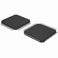
DP83849CVS/NOPB National Semiconductor, DP83849CVS/NOPB Datasheet - Page 57

DP83849CVS/NOPB
Manufacturer Part Number
DP83849CVS/NOPB
Description
IC TXRX ETHERNET PHY DUAL 80TQFP
Manufacturer
National Semiconductor
Type
Transceiverr
Specifications of DP83849CVS/NOPB
Number Of Drivers/receivers
2/2
Protocol
Ethernet
Voltage - Supply
3 V ~ 3.6 V
Mounting Type
Surface Mount
Package / Case
80-TQFP, 80-VQFP
Data Rate
100Mbps
Supply Voltage Range
3V To 3.6V
Logic Case Style
TQFP
No. Of Pins
80
Operating Temperature Range
0°C To +70°C
Msl
MSL 3 - 168 Hours
Filter Terminals
SMD
Rohs Compliant
Yes
Data Rate Max
10Mbps
For Use With
DP83849CVS-EVK - BOARD EVALUATION DP83849CVS
Lead Free Status / RoHS Status
Lead free / RoHS Compliant
Other names
*DP83849CVS
*DP83849CVS/NOPB
DP83849CVS
*DP83849CVS/NOPB
DP83849CVS
Available stocks
Company
Part Number
Manufacturer
Quantity
Price
Company:
Part Number:
DP83849CVS/NOPB
Manufacturer:
NS
Quantity:
618
Company:
Part Number:
DP83849CVS/NOPB
Manufacturer:
Texas Instruments
Quantity:
10 000
7.1.10 PHY Status Register (PHYSTS)
This register provides a single location within the register set for quick access to commonly accessed information.
Bit
15
14
13
12
11
10
9
8
7
POLARITY STATUS
RECEIVE ERROR
PAGE RECEIVED
FALSE CARRIER
SIGNAL DETECT
DESCRAMBLER
MII INTERRUPT
SENSE LATCH
MDIX MODE
RESERVED
Bit Name
LATCH
LOCK
Table 29. PHY Status Register (PHYSTS), address 10h
0, RO/LH
0, RO/LH
0, RO/LL
0, RO/LL
Default
0, RO
0, RO
0, RO
0, RO
0, RO
RESERVED: Write ignored, read as 0.
MDIX mode as reported by the Auto-Negotiation logic:
This bit will be affected by the settings of the MDIX_EN and
FORCE_MDIX bits in the PHYCR register. When MDIX is enabled,
but not forced, this bit will update dynamically as the Auto-MDIX al-
gorithm swaps between MDI and MDIX configurations.
1 = MDI pairs swapped
0 = MDI pairs normal
Receive Error Latch:
This bit will be cleared upon a read of the RECR register.
1 = Receive error event has occurred since last read of RXERCNT
(address 15h, Page 0).
0 = No receive error event has occurred.
Polarity Status:
This bit is a duplication of bit 4 in the 10BTSCR register. This bit will
be cleared upon a read of the 10BTSCR register, but not upon a
read of the PHYSTS register.
1 = Inverted Polarity detected.
0 = Correct Polarity detected.
False Carrier Sense Latch:
This bit will be cleared upon a read of the FCSR register.
1 = False Carrier event has occurred since last read of FCSCR (ad-
dress 14h).
0 = No False Carrier event has occurred.
100Base-TX qualified Signal Detect from PMA:
This is the SD that goes into the link monitor. It is the AND of raw
SD and descrambler lock, when address 16h, bit 8 (page 0) is set.
When this bit is cleared, it will be equivalent to the raw SD from the
PMD.
100Base-TX Descrambler Lock from PMD.
Link Code Word Page Received:
This is a duplicate of the Page Received bit in the ANER register,
but this bit will not be cleared upon a read of the PHYSTS register.
1 = A new Link Code Word Page has been received. Cleared on
read of the ANER (address 06h, bit 1).
0 = Link Code Word Page has not been received.
MII Interrupt Pending:
1 = Indicates that an internal interrupt is pending. Interrupt source
can be determined by reading the MISR Register (12h). Reading
the MISR will clear the Interrupt.
0 = No interrupt pending.
(Receive on TPTD pair, Transmit on TPRD pair)
(Receive on TRD pair, Transmit on TPTD pair)
57
Description
www.national.com


