DP83849CVS/NOPB National Semiconductor, DP83849CVS/NOPB Datasheet - Page 73
DP83849CVS/NOPB
Manufacturer Part Number
DP83849CVS/NOPB
Description
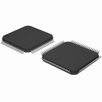
IC TXRX ETHERNET PHY DUAL 80TQFP
Manufacturer
National Semiconductor
Type
Transceiverr
Specifications of DP83849CVS/NOPB
Number Of Drivers/receivers
2/2
Protocol
Ethernet
Voltage - Supply
3 V ~ 3.6 V
Mounting Type
Surface Mount
Package / Case
80-TQFP, 80-VQFP
Data Rate
100Mbps
Supply Voltage Range
3V To 3.6V
Logic Case Style
TQFP
No. Of Pins
80
Operating Temperature Range
0°C To +70°C
Msl
MSL 3 - 168 Hours
Filter Terminals
SMD
Rohs Compliant
Yes
Data Rate Max
10Mbps
For Use With
DP83849CVS-EVK - BOARD EVALUATION DP83849CVS
Lead Free Status / RoHS Status
Lead free / RoHS Compliant
Other names
*DP83849CVS
*DP83849CVS/NOPB
DP83849CVS
*DP83849CVS/NOPB
DP83849CVS
Available stocks
Company
Part Number
Manufacturer
Quantity
Price
Company:

Part Number:
DP83849CVS/NOPB
Manufacturer:
NS
Quantity:
618
Company:
Part Number:
DP83849CVS/NOPB
Manufacturer:
Texas Instruments
Quantity:
10 000


7.3.7 Variance Control Register (VAR_CTRL), Page 2, address 1Ah
The Variance Control and Data Registers provide control and status for the Cable Signal Quality Estimation function.
The Cable Signal Quality Estimation allows a simple method of determining an approximate Signal-to-Noise Ratio for the
100Mb receiver. This register contains the programmable controls and status bits for the variance computation, which
can be used to make a simple Signal-to-Noise Ratio estimation.
7.3.8 Variance Data Register (VAR_DATA), Page 2, address 1Bh
This register contains the 32-bit Variance Sum. The contents of the data are valid only when VAR_RDY is asserted in the
VAR_CTRL register. Upon detection of VAR_RDY asserted, software should set the VAR_FREEZE bit in the VAR_CTRL
register to prevent loading of a new value into the VAR_DATA register. Since the Variance Data value is 32-bits, two
reads of this register are required to get the full value.
14:4
15:0
Bit
2:1
Bit
15
3
0
VAR_FREEZE
VAR_ENABLE
VAR_TIMER
RESERVED
VAR_DATA
VAR_RDY
Bit Name
Bit Name
Table 49. Variance Control Register (VAR_CTRL), address 1Ah
Table 50. Variance Data Register (VAR_DATA), address 1Bh
Default
Default
0, RW
0, RW
0, RW
0, RO
0, RO
0, RO
Variance Data Ready Status:
Indicates new data is available in the Variance data register. This
bit will be automatically cleared after two consecutive reads ot
VAR_DATA.
RESERVED: Writes ignored, read as 0.
Freeze Variance Registers:
Freeze VAR_DATA register.
This bit is ensures that VAR_DATA register is frozen for software
reads. This bit is automatically cleared after two consecutive reads
of VAR_DATA.
Variance Computation Timer (in ms):
Selects the Variance computation timer period. After a new value
is written, computation is automatically restarted. New variance
register values are loaded after the timer elapses.
Var_Timer = 0 => 2 ms timer (default)
Var_Timer = 1 => 4 ms timer
Var_Timer = 2 => 6 ms timer
Var_Timer = 3 => 8 ms timer
Time units are actually 2
Variance Enable:
Enable Variance computation. Off by default.
Variance Data:
Two reads are required to return the full 32-bit Variance Sum value.
Following setting the VAR_FREEZE control, the first read of this
register will return the low 16 bits of the Variance data. A second
read will return the high 16 bits of Variance data.
73
17
Description
Description
cycles of an 8ns clock, or 1.048576ms.
www.national.com
Related parts for DP83849CVS/NOPB
Image
Part Number
Description
Manufacturer
Datasheet
Request
R

Part Number:
Description:
National Semiconductor [8-Bit D/A Converter]
Manufacturer:
National Semiconductor
Datasheet:
Part Number:
Description:
National Semiconductor [Media Coprocessor]
Manufacturer:
National Semiconductor
Datasheet:
Part Number:
Description:
Digitally Controlled Tone and Volume Circuit with Stereo Audio Power Amplifier, Microphone Preamp Stage and National 3D Sound
Manufacturer:
National Semiconductor
Datasheet:
Part Number:
Description:
Digitally Controlled Tone and Volume Circuit with Stereo Audio Power Amplifier, Microphone Preamp Stage and National 3D Sound
Manufacturer:
National Semiconductor
Datasheet:
Part Number:
Description:
AC97 Rev 2 Codec with Sample Rate Conversion and National 3D Sound
Manufacturer:
National Semiconductor
Part Number:
Description:
Manufacturer:
National Semiconductor
Datasheet:
Part Number:
Description:
Manufacturer:
National Semiconductor
Datasheet:
Part Number:
Description:
General Purpose, Low Voltage, Low Power, Rail-to-Rail Output Operational Amplifiers
Manufacturer:
National Semiconductor
Datasheet:
Part Number:
Description:
8-bit 20 MSPS flash A/D converter.
Manufacturer:
National Semiconductor
Datasheet:
Part Number:
Description:
Low Noise Quad Operational Amplifier
Manufacturer:
National Semiconductor
Datasheet:
Part Number:
Description:
Quad Differential Line Receivers
Manufacturer:
National Semiconductor
Datasheet:
Part Number:
Description:
Quad High Speed Trapezoidal? Bus Transceiver
Manufacturer:
National Semiconductor
Datasheet:
Part Number:
Description:
Dual Line Receiver
Manufacturer:
National Semiconductor
Datasheet:
Part Number:
Description:
TTL to 10k ECL Level Translator with Latch
Manufacturer:
National Semiconductor
Datasheet: