USB3319-GJ-TR SMSC, USB3319-GJ-TR Datasheet
USB3319-GJ-TR
Specifications of USB3319-GJ-TR
Available stocks


Related parts for USB3319-GJ-TR


USB3319-GJ-TR Summary of contents
Page 1
... VFBGA lead-free RoHS compliant package also available 0.88mm height) Applications The USB3319 is targeted for any application where a Hi- Speed USB connection is desired and when board space, power, and interface pins must be minimized. The USB3319 is well suited for: ...
Page 2
... USB3319C-CP-TR FOR 24 PIN, QFN LEAD-FREE ROHS COMPLIANT PACKAGE (TAPE AND REEL) USB3319C-GJ-TR FOR 25 PIN, VFBGA LEAD-FREE ROHS COMPLIANT PACKAGE (TAPE AND REEL) This product meets the halogen maximum concentration values per IEC61249-2-21 For RoHS compliance and environmental information, please visit 80 ARKAY DRIVE, HAUPPAUGE, NY 11788 (631) 435-6000, FAX (631) 273-3123 Copyright © ...
Page 3
... It is designed to be used in both commercial and industrial temperature applications. The USB3319 meets all of the electrical requirements to be used as a Hi-Speed USB Host, Device On-the-Go (OTG) device. In addition to the supporting USB signaling the USB3319 also provides USB UART mode and USB Audio mode ...
Page 4
... In USB audio mode, the DP pin is shorted to the SPKR_R/M pin with a switch. The DM pin is shorted to the SPKR_L pin. These switches are on when the RESETB pin of the USB3319 is asserted. Audio signals may be transferred over the USB cable. In addition to audio signals, the switches can also be used to connect Full Speed USB from another PHY onto the USB cable ...
Page 5
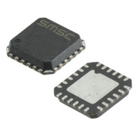
... USB3319 Pin Locations and Descriptions Package Diagram with Pin Locations The pinout below is viewed from the top of the package. ID VBUS VBAT VDD3 Figure 1.1 USB3319 QFN Pinout - Top View Figure 2 USB3319 VFBGA Pinout - Top View SMSC USB3319 REV 24Pin QFN 3 16 4x4mm ...
Page 6
... Power N/A 3.3V Regulator Output. A 2.2uF (<1 ohm ESR) bypass capacitor to ground is required for regulator stability. The bypass capacitor should be placed as close as possible to the USB3319. I/O, N/A D- pin of the USB cable. Analog I/O, N/A D+ pin of the USB cable. ...
Page 7
... USB3319. Input, Low When low, the part is suspended with all CMOS, of the I/O tri-stated. When high the USB3319 will operate as a normal ULPI device. Input, N/A 13MHz Reference Clock input. CMOS Analog, N/A Bias Resistor pin ...
Page 8
... R . VBUS USB C Receptacle 1 VBUS SHIELD GND C DC_BLOCK Figure 3 USB3319 BGA Application Diagram (Device) Revision 2.1 (06-10-10) Hi-Speed USB Transceiver with 1.8V ULPI Interface - 13MHz Reference Clock USB331X DATA7 DATA6 DATA5 DATA4 R VBUS DATA3 C1 VBUS DATA2 DATA1 DATA0 STP ...
Page 9
... VBUS installed on this side VBUS USB C Receptacle 1 VBUS GND SHIELD Figure 3.1 USB3319 QFN Application Diagram (Host or OTG) SMSC USB3319 REV C Voltage at the VBUS pin must not be allowed to exceed V . VMAX USB331X DATA7 DATA6 DATA5 DATA4 R VBUS DATA3 2 VBUS DATA2 DATA1 ...
Page 10
... VBUS USB C Receptacle 1 VBUS GND SHIELD Figure 4 USB3319 BGA Application Diagram (Host or OTG) Revision 2.1 (06-10-10) Hi-Speed USB Transceiver with 1.8V ULPI Interface - 13MHz Reference Clock Voltage at the VBUS pin must not be allowed to exceed V . VMAX USB331X DATA7 DATA6 DATA5 DATA4 R VBUS ...
Page 11
Package Outline Figure 4.1 24-pin QFN, 4x4mm Body, 0.5mm Pitch ...
Page 12
Figure 5 25-Pin VFBGA, 3x3mm Body, 0.5mm Pitch ...