STLVDS3486BDR STMicroelectronics, STLVDS3486BDR Datasheet
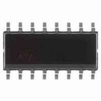
IC RECEIVER HS DIFF LINE 16 SOIC

STLVDS3486BDR

Manufacturer Part Number
STLVDS3486BDR
Description
IC RECEIVER HS DIFF LINE 16 SOIC
Manufacturer
STMicroelectronics
Type
Receiverr
Datasheets

Specifications of STLVDS3486BDR

Number Of Drivers/receivers
0/4
Protocol
RS644
Voltage - Supply
3 V ~ 3.6 V
Mounting Type
Surface Mount
Package / Case
16-SOIC (3.9mm Width)
Number Of Elements
4
Number Of Receivers
4
Number Of Drivers
4
Operating Supply Voltage (typ)
3.3V
Differential Input High Threshold Voltage
100mV
Diff. Input Low Threshold Volt
-100mV
Transmission Data Rate
400Mbps
Propagation Delay Time
3.3ns
Operating Temp Range
-40C to 85C
Operating Temperature Classification
Industrial
Mounting
Surface Mount
Pin Count
16
Package Type
SO
Lead Free Status / RoHS Status
Contains lead / RoHS non-compliant
Other names
497-2149-2

Available stocks

Company
Part Number
Manufacturer
Quantity
Price
Part Number:
STLVDS3486BDR
Manufacturer:
STM
Quantity:
2 478
Part Number:
STLVDS3486BDR
Manufacturer:
ST
0
DESCRIPTION
The STLVDS32 and STLVD3486 are differential
line receivers that implement the electrical
characteristics of low voltage differential signaling
(LVDS). This signaling technique lower the output
voltage levels of 5V differential standard levels
(such as TIA/EIA-422B) to reduce the power,
increase the switching speeds and allows
operations with a 3.3V supply rail. Any of the four
differential receivers provides a valid logical
ORDERING CODES
November 2002
STLVDS3487BDR
STLVDS3487BTR
STLVDS3487BD
STLVDS32BDR
STLVDS32BTR
STLVDS32BD
MEETS OR EXCEEDS THE
REQUIREMENTS OF ANSI TIA/EIA-644
STANDARD
OPERATES WITH A SINGLE 3.3V SUPPLY
DESIGNED FOR SIGNALING RATE UP TO
400Mbps
DIFFERENTIAL INPUT THRESHOLDS
TYPICAL PROPAGATION DELAY TIME OF
2.5ns
POWER DISSIPATION 60mW TYPICAL PER
RECEIVER AT 200MHz
LOW VOLATGE TTL (LVTTL) LOGIC
OUTPUT LEVELS
PIN COMPATIBLE WITH THE AM26LS32,
SN65LVD32, MC3486 AND SN65LVD3486
OPEN CIRCUIT FAIL SAFE
7KV BUS PIN ESD PROTECTION
3KV ALL PINS VS GND
100mV MAX
Type
Temperature
-40 to 85 C
-40 to 85 C
-40 to 85 C
-40 to 85 C
-40 to 85 C
-40 to 85 C
Range
TSSOP16 (Tape & Reel)
SO-16 (Tape & Reel)
SO-16 (Tape & Reel)
SO-16 (Tube)
SO-16 (Tube)
DIFFERENTIAL LINE RECEIVERS
Package
output state with a 3.3V supply rail. Any of the four
differential receivers provides a valid logical
output state with a
voltage within the input common mode voltage
range. The input common mode voltage allows 1V
of ground potential difference between two LVDS
nodes.
The intended application of this device and
signalling technique is both point-to-point and
multidrop data transmission over controlled
impedance media approximately 100 . The
transmission media may be printed circuit board
traces, backplanes or cables. The ultimate rate
and distance of data transfer is dependent upon
the attenuation characteristics of the media and
noise coupling to the enviroment.
The STLVDS32 and STLVD3486 ”B” version are
characterized for operation from -40 C to 85 C.
SOP
50parts per tube / 20tube per box
STLVDS3486
100mV
2500 parts per reel
2500 parts per reel
2500 parts per reel
2500 parts per reel
STLVDS32
HIGH SPEED
Comments
TSSOP
differential input
1/11

Related parts for STLVDS3486BDR

STLVDS3486BDR Summary of contents

Page 1

MEETS OR EXCEEDS THE REQUIREMENTS OF ANSI TIA/EIA-644 STANDARD OPERATES WITH A SINGLE 3.3V SUPPLY DESIGNED FOR SIGNALING RATE UP TO 400Mbps DIFFERENTIAL INPUT THRESHOLDS 100mV MAX TYPICAL PROPAGATION DELAY TIME OF 2.5ns POWER DISSIPATION 60mW TYPICAL PER RECEIVER AT ...

Page 2

STLVDS32/STLVDS3486 PIN CONFIGURATION STLVDS32 STLVDS32 PIN DESCRIPTION PlN N SYMBOL NAME AND FUNCTION Receiver Inputs Negated Receiver Inputs Receiver ...

Page 3

LOGIC DIAGRAM AND LOGIC SYMBOL FOR STLVDS3486 STLVDS32 TRUTH TABLE DIFFERENTIAL INPUTS 100mV ID -100mV < V < 100mV ID V -100mV ID X OPEN/SHORT or Terminated (Full Fail-Safe) L=Low level, H=High Level, X=Don’t care, Z= High ...

Page 4

STLVDS32/STLVDS3486 ABSOLUTE MAXIMUM RATINGS Symbol V Supply Voltage (Note Input Voltage I V Input Voltage ( inputs) I Human Body Model ESD T Storage Temperature Range stg Absolute Maximum Ratings are those values beyond which ...

Page 5

SWITCHING CHARACTERISTICS (Unless otherwise noted. Typical values are referred to T and V = 3.3V) CC Symbol Parameter t Propagation Delay Time, C PLH Low to High Output t Propagation Delay Time, PHL High to Low Output t Differential Output ...

Page 6

STLVDS32/STLVDS3486 Figure 1 : Timing Test Circuit, Timing And Waveforms Note A: All input pulse are supplied by a generator having the following characteristics: t pulse width = 10 0.2ns. Note B: C includes instrumentation and fixture capacitance within 6mm ...

Page 7

Figure 2 : Enable And Disable Time Test Circuit And Waveform Note A: All input pulse are supplied by a generator having the following characteristics: t pulse width = 500 10ns. Note B: C includes instrumentation and fixture capacitance within ...

Page 8

STLVDS32/STLVDS3486 TYPICAL PERFORMANCE CHARACTERISTICS (unless otherwise specified T Figure 3 : Output Current vs Output Voltage 8/ Figure 4 : Output Current vs Output Voltage ...

Page 9

SO-16 MECHANICAL DATA mm. DIM. MIN. TYP 0.35 b1 0. 9.8 E 5.8 e 1.27 e3 8.89 F 3.8 G 4 STLVDS32/STLVDS3486 inch MAX. MIN. TYP. ...

Page 10

STLVDS32/STLVDS3486 TSSOP16 MECHANICAL DATA DIM. MIN 0.05 A2 0.8 b 0.19 c 0.09 D 4.9 E 6.2 E1 4.3 e 0.65 BSC 0. PIN 1 IDENTIFICATION 1 10/11 mm. TYP MAX. ...

Page 11

... No license is granted by implication or otherwise under any patent or patent rights of STMicroelectronics. Specifications mentioned in this publication are subject to change without notice. This publication supersedes and replaces all information previously supplied ...

Related keywords