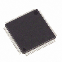
DS2154L+ Maxim Integrated Products, DS2154L+ Datasheet - Page 14

DS2154L+
Manufacturer Part Number
DS2154L+
Description
IC TXRX E1 1CHIP 5V ENH 100-LQFP
Manufacturer
Maxim Integrated Products
Type
Transceiverr
Datasheet
1.DS2154L.pdf
(87 pages)
Specifications of DS2154L+
Number Of Drivers/receivers
1/1
Protocol
E1
Voltage - Supply
4.75 V ~ 5.25 V
Mounting Type
Surface Mount
Package / Case
100-LQFP
Product
Framer
Number Of Transceivers
1
Data Rate
1.544 Mbps
Supply Voltage (max)
5.25 V
Supply Voltage (min)
4.75 V
Supply Current (max)
75 mA (Typ)
Maximum Operating Temperature
+ 70 C
Minimum Operating Temperature
0 C
Mounting Style
SMD/SMT
Ic Interface Type
Parallel, Serial
Supply Voltage Range
4.75V To 5.25V
Operating Temperature Range
0°C To +70°C
Digital Ic Case Style
LQFP
No. Of Pins
100
Filter Terminals
SMD
Rohs Compliant
Yes
Lead Free Status / RoHS Status
Lead free / RoHS Compliant
2.4 Line Interface Pins
2.5 Supply Pins
44, 61,
45, 60,
19, 20,
16, 17
29, 32
81, 83
80, 84
PIN
PIN
21
22
13
12
18
31
24
30
XTALD
8XCLK
RRING
TRING
MCLK
DVDD
NAME
NAME
RVDD
TVDD
DVSS
RVSS
RTIP,
TVSS
LIUC
TTIP,
Master Clock Input. A 2.048MHz (±50ppm) clock source with TTL levels is applied at
this pin. This clock is used internally for both clock/data recovery and for jitter
attenuation. A quartz crystal of 2.048MHz may be applied across MCLK and XTALD
instead of the TTL level clock source.
Quartz Crystal Driver. A quartz crystal of 2.048MHz may be applied across MCLK
and XTALD instead of a TTL level clock source at MCLK. Leave open circuited if a
TTL clock source is applied at MCLK.
Eight Times Clock. A 16.384MHz clock that is frequency locked to the 2.048MHz
clock provided from the clock/data recovery block (if the jitter attenuator is enabled on
the receive side) or from the TCLKI pin (if the jitter attenuator is enabled on the transmit
side). Can be internally disabled via the TEST2 register if not needed.
Line Interface Connect. Tie low to separate the line interface circuitry from the
framer/formatter circuitry and activate the TPOSI/TNEGI/TCLKI/RPOSI/RNEGI/
RCLKI pins. Tie high to connect the line interface circuitry to the framer/formatter
circuitry and deactivate the TPOSI/TNEGI/TCLKI/RPOSI/RNEGI/RCLKI pins. When
LIUC is tied high, the TPOSI/TNEGI/TCLKI/RPOSI/RNEGI/RCLKI pins should be
tied low.
Receive Tip and Ring. Analog inputs for clock recovery circuitry. These pins connect
via a 1:1 transformer to the E1 line. See Section
Transmit Tip and Ring. Analog line driver outputs. These pins connect via a 1:1.15 or
1:1.36 step-up transformer to the E1 line. See Section
Digital Positive Supply. 5.0V ±5%. Should be tied to the RVDD and TVDD pins.
Receive Analog Positive Supply. 5.0V ±5%. Should be tied to the DVDD and TVDD
pins.
Transmit Analog Positive Supply. 5.0V ±5%. Should be tied to the RVDD and DVDD
pins.
Digital Signal Ground. Should be tied to the RVSS and TVSS pins.
Receive Analog Signal Ground. 0V. Should be tied to the DVSS and TVSS pins.
Transmit Analog Ground. 0V. Should be tied to the RVSS and DVSS pins.
14 of 87
FUNCTION
FUNCTION
13
for details.
13
for details.


