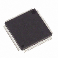
DS2154L+ Maxim Integrated Products, DS2154L+ Datasheet - Page 29

DS2154L+
Manufacturer Part Number
DS2154L+
Description
IC TXRX E1 1CHIP 5V ENH 100-LQFP
Manufacturer
Maxim Integrated Products
Type
Transceiverr
Datasheet
1.DS2154L.pdf
(87 pages)
Specifications of DS2154L+
Number Of Drivers/receivers
1/1
Protocol
E1
Voltage - Supply
4.75 V ~ 5.25 V
Mounting Type
Surface Mount
Package / Case
100-LQFP
Product
Framer
Number Of Transceivers
1
Data Rate
1.544 Mbps
Supply Voltage (max)
5.25 V
Supply Voltage (min)
4.75 V
Supply Current (max)
75 mA (Typ)
Maximum Operating Temperature
+ 70 C
Minimum Operating Temperature
0 C
Mounting Style
SMD/SMT
Ic Interface Type
Parallel, Serial
Supply Voltage Range
4.75V To 5.25V
Operating Temperature Range
0°C To +70°C
Digital Ic Case Style
LQFP
No. Of Pins
100
Filter Terminals
SMD
Rohs Compliant
Yes
Lead Free Status / RoHS Status
Lead free / RoHS Compliant
CCR5: COMMON CONTROL REGISTER 5 (Address = AA Hex)
4.1 Framer Loopback
When CCR1.7 is set to 1, the DS2154 enters a Framer Loopback (FLB) mode. See
This loopback is useful in testing and debugging applications. In FLB, the DS2154 loops data from the
transmit side back to the receive side. When FLB is enabled, the following occurs:
1) Data is transmitted as normal at TPOSO and TNEGO.
2) Data input via RPOSI and RNEGI is ignored.
3) The RCLK output is replaced with the TCLK input.
4.2 Local Loopback
When CCR4.6 is set to 1, the DS2154 is forced into Local Loopback (LLB). In this loopback, data
continues to be transmitted as normal through the transmit side of the DS2154. Data being received at
RTIP and RRING is replaced with the data being transmitted. Data in this loopback passes through the
jitter attenuator. See
4.3 Remote Loopback
When CCR4.7 is set to 1, the DS2154 is forced into Remote Loopback (RLB). In this loopback, data
input via the RPOSI and RNEGI pins is transmitted back to the TPOSO and TNEGO pins. Data continues
to pass through the receive side framer of the DS2154 as it would normally, and the data from the
transmit side formatter is ignored. See
(MSB)
LIRST
SYMBOL
LIRST
RCM4
RCM3
RCM2
RCM1
RCM0
—
—
Figure 1-1
POSITION
CCR5.6,
CCR5.7
CCR5.5
CCR5.4
CCR5.3
CCR5.2
CCR5.1
CCR5.0
—
for more details.
Figure 1-1
NAME AND DESCRIPTION
Line Interface Reset. Setting this bit from a 0 to a 1 will initiate
an internal reset that affects the clock recovery state machine and
jitter attenuator. Normally this bit is only toggled on power-up.
Must be cleared and set again for a subsequent reset.
Not Assigned. Should be set to 0 when written.
Receive Channel Monitor Bit 4. MSB of a channel decode that
determines which receive channel data will appear in the
RDS0M register. See Section
Receive Channel Monitor Bit 3.
Receive Channel Monitor Bit 2.
Receive Channel Monitor Bit 1.
Receive Channel Monitor Bit 0. LSB of the channel decode.
RCM4
29 of 87
for more details.
RCM3
RCM2
7
for details.
RCM1
Figure 1-1
for details.
RCM0
(LSB)


