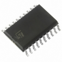
L6374FP STMicroelectronics, L6374FP Datasheet

L6374FP
Specifications of L6374FP
Available stocks
Related parts for L6374FP
L6374FP Summary of contents
Page 1
... SO-20 Description The L6374 is especially designed to be used as a line driver in industrial control systems based on the 24 V signal levels (IEC 61131, 24VDC). Table 1. Device summary Order codes Package L6374FP SO-20 L6374FPT SO-20 Rev 3 L6374 Packaging Tube Tape and reel 1/19 www.st.com 19 ...
Page 2
Contents Contents 1 Maximum ratings . . . . . . . . . . . . . . . . . . . . . . . . . . . . . . . . . . . ...
Page 3
L6374 1 Maximum ratings Table 2. Absolute maximum ratings Symbol Pin 12, ilog 13 I ilog out 17 out I set 11 V ...
Page 4
Electrical characteristics 3 Electrical characteristics Table 3. Electrical characteristics Symbol Pin Parameter DC operation ( -25 to 125 °C; unless otherwise specified Supply voltage upperthreshold ...
Page 5
L6374 Table 3. Electrical characteristics (continued) Symbol Pin Parameter AC operation ( waveforms diagrams Delay time on rising edge to181 Delay ...
Page 6
Thermal characteristics 4 Thermal characteristics Table 4. Thermal data Symbol R Thermal resistance, junction to pin thJP Thermal resistance, junction to ambient R thJA1 (see thermal characteristics) Thermal resistance, junction to ambient R thJA2 (see thermal characteristics) 4.1 R thJP ...
Page 7
L6374 Figure 3. Printed heatsink Thermal characteristics 7/19 ...
Page 8
Overtemperature protection (OVT) 5 Overtemperature protection (OVT) If the chip temperature exceeds T deactivates itself. The following actions are taken: ● all the output stages are forced in the "three state" condition, i.e. are disconnected from the output pins; only ...
Page 9
L6374 7 Diagnostic logic The situations that are monitored and signalled with the Diag output pin are: ● current limit (OVC) in action; there are 8 individual current limiting circuits, two per each output, i.e. one per every output transistor; ...
Page 10
State / push-pull input 10 State / push-pull input The input 3st/Pp is instead intended for a digital incoming signal. It has an internal threshold set at 1. internal bias circuit (10 mA typical) simulates a high level ...
Page 11
L6374 11 The switching of the output stage The cross conduction of the two transistors of an output stage of the L6374 would be significantly noisy, because the transistors here can carry peak currents in excess of 100 mA, and ...
Page 12
The switching of the output stage switching when the inductor can discharge; while the switching looks "delayed" if the output transition tends to initiate a charging phase (see parasitic elements, the waveforms resemble the ones of the purely resistive cases. ...
Page 13
L6374 = 35 V, 350 Ω connected to V Figure 350 Ω and 1 mH connected to ground. Figure The switching of the output stage S 13/19 ...
Page 14
The switching of the output stage = 35 V, 350 Ω connected to ground. Figure 10 Figure 11. Switching waveforms. In Out 14/19 50 90% 10 L6374 50 ...
Page 15
L6374 12 Application note It is recommended not to leave the Ref pin (pin 11) floating: if not used with an external voltage reference better to connect an external capacitor (of at least 10 nF) between this pin ...
Page 16
Package mechanical data 13 Package mechanical data In order to meet environmental requirements, ST offers these devices in ECOPACK® packages. These packages have a lead-free second level interconnect . The category of second level interconnect is marked on the package ...
Page 17
L6374 Table 5. SO-20 mechanical data Dim Figure 12. Package dimensions mm Min Typ Max 2.35 2.65 0.1 0.3 0.33 0.51 0.23 0.32 12.6 13 7.4 7.6 1.27 10 ...
Page 18
Revision history 14 Revision history Table 6. Document revision history Date August 2003 June 2004 03-Mar-2008 18/19 Revision 1 First Issue 2 Technical migration from ST-PRESS to EDOCS. 3 Modified: Removed obsolete package DIP-20 L6374 Changes ...
Page 19
... L6374 Information in this document is provided solely in connection with ST products. STMicroelectronics NV and its subsidiaries (“ST”) reserve the right to make changes, corrections, modifications or improvements, to this document, and the products and services described herein at any time, without notice. All ST products are sold pursuant to ST’s terms and conditions of sale. ...


