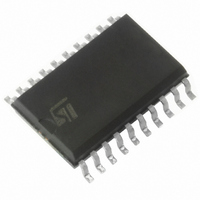
L6374FP STMicroelectronics, L6374FP Datasheet - Page 8

L6374FP
Manufacturer Part Number
L6374FP
Description
IC LINE DRIVER QUAD IND 20-SOIC
Manufacturer
STMicroelectronics
Type
Driverr
Datasheet
1.L6374FP013TR.pdf
(19 pages)
Specifications of L6374FP
Number Of Drivers/receivers
4/0
Voltage - Supply
10.8 V ~ 35 V
Mounting Type
Surface Mount
Package / Case
20-SOIC (7.5mm Width)
Supply Voltage (max)
35 V
Supply Voltage (min)
10.8 V
Maximum Operating Temperature
+ 85 C
Mounting Style
SMD/SMT
Minimum Operating Temperature
- 25 C
Supply Current
5000 uA
Lead Free Status / RoHS Status
Lead free / RoHS Compliant
Protocol
-
Lead Free Status / Rohs Status
Details
Available stocks
Company
Part Number
Manufacturer
Quantity
Price
Overtemperature protection (OVT)
5
6
8/19
Overtemperature protection (OVT)
If the chip temperature exceeds T
deactivates itself.
The following actions are taken:
●
●
Normal operation is resumed as soon as (typically after some seconds) the chip
temperature monitored goes back below T
The different upper and lower thresholds with hysteretic behavior, assure that no intermittent
conditions can be generated.
Undervoltage protection (UV)
The supply voltage is expected to range from 11 V to 35 V, even if its reference value is
considered to be 24 V.
In this range the L6374 operates correctly. Below 10.8 V the overall system has to be
considered not reliable.
Consequently the supply voltage is monitored continuously and a signal, called UV, is
internally generated and used.
The signal is "on" as long as the supply voltage does not reach the upper internal threshold
of the V
Once the UV signal has been removed, the supply voltage must decrease below the lower
threshold (i.e. below V
The hysteresis H
voltages that may have a superimposed ripple around the average value.
The UV signal inhibits the outputs, putting them in three-state, but has no effect on the
creation of the reference voltages for the internal comparators, nor on the continuous
operation of the charge-pump circuits.
all the output stages are forced in the "three state" condition, i.e. are disconnected from
the output pins; only the clamping diodes at the outputs remain active;
the signal Diag is activated (active low).
s
comparator (called V
ys1
is provided to prevent intermittent operation of the device at low supply
sh
-H
ys1
) before it is turned on again.
sh
). The UV signal disappears above V
h
(measured in a central position in the chip) the chip
h
-H
T
.
sh
.
L6374


