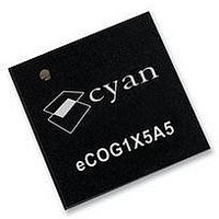
ECOG1X5A5L CYAN, ECOG1X5A5L Datasheet - Page 20

ECOG1X5A5L
Manufacturer Part Number
ECOG1X5A5L
Description
MCU, 16BIT, 512K FLASH, USB, 68QFN
Manufacturer
CYAN
Datasheet
1.ECOG1X5A5L.pdf
(95 pages)
Specifications of ECOG1X5A5L
Core Size
16bit
No. Of I/o's
32
Program Memory Size
512KB
Ram Memory Size
24KB
Cpu Speed
70MHz
Oscillator Type
External, Internal
No. Of Timers
5
No. Of Pwm Channels
2
Rohs Compliant
Yes
Controller Family/series
ECOG1X
Version 1.17
Operating Modes
Instruction Cache
Memory Management Unit
20
There are three independent aspects of the processor operating modes.
Processor State
When the processor is awake, it fetches and executes instructions normally. When the processor is
asleep, no instructions are executed. The SLEEP instruction changes from the awake to the asleep
state, and selected peripherals are stopped automatically to reduce power consumption. External I/O
activity triggers a wake up event, and selected peripherals are started automatically.
Processor Mode
Interrupts from internal or external peripherals are enabled in user mode. When an interrupt is
serviced, the processor changes from user to interrupt mode. No further interrupts are serviced until
the processor completes the current interrupt service routine and returns with an RTI instruction.
In user mode, the processor uses the UX and UY registers. In interrupt mode, it uses the IX and IY
registers. It is possible to switch between user and interrupt modes in software by changing the state of
the interrupt mode bit in the flags register.
Program State
When executing an application, the program is in the normal running state. When debug mode is
enabled via the eICE debug port, the program can change to the stopped state on the following events.
•
•
•
•
Once the program is stopped, a run command received via the eICE debug port restarts execution.
The eCOG1X has an on-chip instruction cache, implemented using fast SRAM. This fast memory area
can be configured as a direct mapped four word 256 line instruction cache, or as an additional 1280
words of on-chip SRAM. The cache increases the processing speed when executing code from flash
memory, and reduces the power consumption.
The instruction cache also provides support for large numbers of breakpoints when debugging. Many
BRK instructions can be locked in the cache as soft breakpoints, even when executing code from
internal flash memory.
The Memory Management Unit (MMU) allows a variety of internal and external memories to be
combined into a single logical memory structure. The memory structure or model has both code space
and data space address locations to match the Harvard architecture CPU. The MMU provides both
code space translations for program code and data space translations for variables and constants. A
single physical memory can be mapped into both code and data space.
Processor State
Processor Mode
Program State
A BRK instruction is executed.
The PC register becomes equal to one of the code address breakpoint registers.
A data space access matches the configuration in the data breakpoint registers.
An eICE stop command is received via the debug port.
eCOG and CyanIDE are registered trademarks of Cyan Holdings plc
awake or asleep
interrupt or user mode
running or stopped (used when debugging)
eCOG1X Microcontroller Product Family
www.cyantechnology.com
11 February 2010


