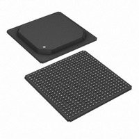
DS32508N+ Maxim Integrated Products, DS32508N+ Datasheet - Page 43

DS32508N+
Manufacturer Part Number
DS32508N+
Description
IC LIU DS3/E3/STS-1 484-BGA
Manufacturer
Maxim Integrated Products
Type
Line Interface Units (LIUs)r
Datasheet
1.DS32506N.pdf
(130 pages)
Specifications of DS32508N+
Protocol
IEEE 1149.1
Voltage - Supply
1.8V, 3.3V
Mounting Type
Surface Mount
Package / Case
484-BGA
Lead Free Status / RoHS Status
Lead free / RoHS Compliant
Number Of Drivers/receivers
-
goes low. The PMS has an associated latched status bit that can generate an interrupt if enabled. The port PMS
signal does not go high until an update of all the appropriately configured block-level performance monitoring
counters in the port has been completed. The global PMS signal does not go high until an update of all the
appropriately configured port-level performance monitoring counters in the entire chip has been completed.
8.7.5 Transmit Manual Error Insertion
Various types of errors can be inserted in the transmit data stream using the Transmit Manual Error Insertion
(TMEI) signal, which can be sourced from a block-level register bit, a port register bit (PORT.CR1:TMEI), a global
register bit (GLOBAL.CR1:TMEI), or a general-purpose I/O pin (GPIOB2). To use GPIOB2 as the TMEI signal,
GLOBAL.CR1.MEIMS is set to 1, the appropriate PORT.CR1.MEIMS bits are set to 1, and the appropriate block-
level MEIMS bits are set to 1. To use the global TMEI register bit, GLOBAL.CR1.MEIMS is set to 0, the appropriate
PORT.CR1.MEIMS bits are set to 1, and the appropriate block-level MEIMS bits are set to 1. To use the port TMEI
register bit, the associated PORT.CR1.MEIMS is set to 0 and the appropriate block-level MEIMS bits are set to 1.
To use the block-level TSEI register bit, the associated block-level MEIMS bit is set to 0.
In order for an error of a particular type to be inserted, the error type must be enabled by setting the associated
error insertion enable bit in the associated block's error insertion register. Once enabled, a single error is inserted
at the next opportunity when the TMEI signal transitions from zero to one. Note: If the TMEI signal has multiple
zero-to-one transitions between error insertion opportunities, only a single error is inserted.
8.8 8-/16-Bit Parallel Microprocessor Interface
See
8.8.1 8-Bit and 16-Bit Bus Widths
When the
(IFSEL
used, and the upper 8 data lines D[15:8] are disabled (high impedance). In 16-bit modes
address does not include A[0], and all 16 data lines
8.8.2
In 16-bit modes
used to determine whether byte swapping is enabled. This pin should be static and not change during operation.
When the
D[15:8], and the lower register bits REG[7:0] are mapped to the lower external data bus lines D[7:0]. When the
BSWAP
the lower register bits REG[7:0] are mapped to the upper external data bus lines D[15:8].
8.8.3 Read-Write And Data Strobe Modes
The processor interface can operate in either read-write strobe mode (also known as "Intel" mode) or data strobe
mode (also known as "Motorola" mode). When
negative pulse on
When
performs a read cycle, and a negative pulse on
8.8.4 Multiplexed and Nonmultiplexed Operation
In all parallel interface modes the interface supports both multiplexed and nonmultiplexed operation. For
multiplexed operation in 8-bit modes, wire A[10:8] to the processor’s A[10:8] pins, wire A[7:0] to D[7:0] and to the
processor’s multiplexed address/data bus, and connect the
nonmultiplexed 8-bit operation, wire
For multiplexed operation in 16-bit modes, wire A[10:0] to D[10:0], wire
address/data bus, and connect the
operation, wire
Table 11-8
IFSEL
= 10X), the address is composed of all the address bits including A[0], the lower 8 data lines D[7:0] are
Byte Swap Mode
pin is high the upper register bits REG[15:8] are mapped to the lower external data bus lines D[7:0], and
BSWAP
IFSEL
= 1X1 the data strobe mode is enabled. In this mode, a negative pulse on
ALE
and
(IFSEL
RD
pins are set to 1XX, the device presents a parallel microprocessor interface. In 8-bit modes
pin is low the upper register bits REG[15:8] are mapped to the upper external data bus lines
high and wire A[10:0] and
Figure 11-3
performs a read cycle, and a negative pulse on
= 11X), the microprocessor interface can operate in byte swap mode. The
to
Figure 11-10
ALE
ALE
high and wire A[10:0] and D[7:0] to the appropriate pins on the processor.
pin to the appropriate pin on the processor. For nonmultiplexed 16-bit
D[15:0]
IFSEL
DS
for parallel interface timing diagrams and parameters.
when
D[15:0]
43 of 130
to the appropriate pins on the processor.
= 1X0 the read-write strobe mode is enabled. In this mode a
R/W
are used.
ALE
is low performs a write cycle.
pin to the appropriate pin on the processor. For
WR
performs a write cycle.
D[15:0]
DS32506/DS32508/DS32512
to the CPU’s multiplexed
DS
(IFSEL
when
BSWAP
= 11X), the
R/W
is high
pin is


