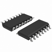
PTN3332D,112 NXP Semiconductors, PTN3332D,112 Datasheet - Page 12

PTN3332D,112
Manufacturer Part Number
PTN3332D,112
Description
IC DIFF LINE RCVR 16SOIC
Manufacturer
NXP Semiconductors
Type
Transceiverr
Datasheet
1.PTN3332D112.pdf
(16 pages)
Specifications of PTN3332D,112
Number Of Drivers/receivers
4/0
Protocol
RS644
Voltage - Supply
3 V ~ 3.6 V
Mounting Type
Surface Mount
Package / Case
16-SOIC (3.9mm Width)
Lead Free Status / RoHS Status
Lead free / RoHS Compliant
Other names
935271102112
PTN3332D
PTN3332D
PTN3332D
PTN3332D
Philips Semiconductors
14. Soldering
PTN3332_2
Product data sheet
14.1 Introduction to soldering surface mount packages
14.2 Reflow soldering
14.3 Wave soldering
There is no soldering method that is ideal for all surface mount IC packages. Wave
soldering can still be used for certain surface mount ICs, but it is not suitable for fine pitch
SMDs. In these situations reflow soldering is recommended.
Reflow soldering requires solder paste (a suspension of fine solder particles, flux and
binding agent) to be applied to the printed-circuit board by screen printing, stencilling or
pressure-syringe dispensing before package placement. Driven by legislation and
environmental forces the worldwide use of lead-free solder pastes is increasing.
Several methods exist for reflowing; for example, convection or convection/infrared
heating in a conveyor type oven. Throughput times (preheating, soldering and cooling)
vary between 100 seconds and 200 seconds depending on heating method.
Typical reflow temperatures range from 215 C to 260 C depending on solder paste
material. The peak top-surface temperature of the packages should be kept below:
Table 9.
Table 10.
Moisture sensitivity precautions, as indicated on packing, must be respected at all times.
Conventional single wave soldering is not recommended for surface mount devices
(SMDs) or printed-circuit boards with a high component density, as solder bridging and
non-wetting can present major problems.
To overcome these problems the double-wave soldering method was specifically
developed.
If wave soldering is used the following conditions must be observed for optimal results:
Package thickness
< 2.5 mm
Package thickness
< 1.6 mm
1.6 mm to 2.5 mm
•
•
2.5 mm
2.5 mm
Use a double-wave soldering method comprising a turbulent wave with high upward
pressure followed by a smooth laminar wave.
For packages with leads on two sides and a pitch (e):
July 2004)
2004)
SnPb eutectic process - package peak reflow temperatures (from J-STD-020C
Pb-free process - package peak reflow temperatures (from J-STD-020C July
Rev. 02 — 14 August 2006
Volume mm
260 C + 0 C
260 C + 0 C
250 C + 0 C
Volume mm
240 C + 0/ 5 C
225 C + 0/ 5 C
3
< 350
3
< 350
Volume mm
2000
260 C + 0 C
250 C + 0 C
245 C + 0 C
High speed differential line receiver
3
350 to
© Koninklijke Philips Electronics N.V. 2006. All rights reserved.
Volume mm
225 C + 0/ 5 C
225 C + 0/ 5 C
Volume mm
260 C + 0 C
245 C + 0 C
245 C + 0 C
PTN3332
3
350
3
> 2000
12 of 16


