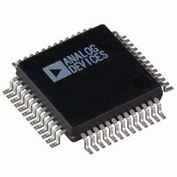
ADV7195KS Analog Devices Inc, ADV7195KS Datasheet - Page 18

ADV7195KS
Manufacturer Part Number
ADV7195KS
Description
IC DAC VID-HDTV 3CH-11BIT 52MQFP
Manufacturer
Analog Devices Inc
Type
Video Encoderr
Datasheet
1.ADV7195KS.pdf
(36 pages)
Specifications of ADV7195KS
Rohs Status
RoHS non-compliant
Applications
HDTV, MPEG, Image Processing
Voltage - Supply, Analog
3.3V
Voltage - Supply, Digital
3.3V
Mounting Type
Surface Mount
Package / Case
52-MQFP, 52-PQFP
Adc/dac Resolution
11b
Screening Level
Commercial
Package Type
MQFP
Pin Count
52
For Use With
EVAL-ADV7195EB - BOARD EVAL FOR ADV7195
Lead Free Status / RoHS Status
Not Compliant
Available stocks
Company
Part Number
Manufacturer
Quantity
Price
Part Number:
ADV7195KSZ
Manufacturer:
ADI/亚德诺
Quantity:
20 000
MODE REGISTER 3
MR3 (MR37–MR30)
(Address (SR4–SR0) = 03H)
Figure 23 shows the various operations under the control of
Mode Register 3.
MR3 BIT DESCRIPTION
HDTV Enable (MR30)
When this bit is set to “1,” the ADV7195 reverts to HDTV mode
(refer to HDTV mode section). When set to “0” the ADV7195
is set up in Progressive Scan Mode (PS Mode).
Reserved (MR31–MR32)
A “0” must be written to these bits.
DAC A Control (MR33)
Setting this bit to “1” enables DAC A, otherwise this DAC is
powered down.
DAC B Control (MR34)
Setting this bit to “1” enables DAC B, otherwise this DAC is
powered down.
DAC C Control (MR35)
Setting this bit to “1” enables DAC C, otherwise this DAC is
powered down.
Interpolation (MR36)
This bit enables the second stage interpolation filters. When this
bit is enabled (MR36 = “1”), data is sent at 54 MHz to the DAC
output stage. After Reset it is recommended to toggle this bit.
Before toggling this bit, 3Ehex must be written to address 09hex
to guarantee correct operation.
Reserved (MR37)
A “0” must be written to this bit.
ADV7195
ZERO MUST BE
MR36
WRITTEN TO
INTERPOLATION
0
1
THIS BIT
MR47
MR37
MR37
DISABLE
ENABLE
MR46
MR36
MR35
0
1
DAC C CONTROL
MR45
ZERO MUST BE
MR35
POWER-DOWN
NORMAL
MR47 – MR41
WRITTEN TO
THESE BITS
MR34
DAC B CONTROL
0
1
MR44
POWER-DOWN
NORMAL
MR34
MR33
0
1
DAC A CONTROL
MR43
MODE REGISTER 4
MR4 (MR47–MR40)
(Address (SR4–SR0) = 04H)
Figure 24 shows the various operations under the control of
Mode Register 4.
MR4 BIT DESCRIPTION
Timing Reset (MR40)
Toggling MR40 from low to high and low again resets the inter-
nal horizontal and vertical timing counters.
MODE REGISTER 5
MR5 (MR57–MR50)
(Address (SR4-SR0) = 05H)
Figure 25 shows the various operations under the control of
Mode Register 5.
MR5 BIT DESCRIPTION
Reserved (MR50)
This bit is reserved for the revision code.
RGB Mode (MR51)
When RGB mode is enabled (MR51 = “1”) the ADV7195
accepts unsigned binary RGB data at its input port. This control
is also available in Async Timing Mode.
Sync on PrPb (MR52)
By default, the color component output signals Pr, Pb do not
contain any horizontal sync pulses. They can be inserted when
MR52 = “1.” This facility is only available when Output Stan-
dard Selection has been set to EIA-770.2 (MR01–00 = “00”) or
Full Input Range (MR01–00 = “10”).
This control is not available in RGB mode.
MR33
POWER-DOWN
NORMAL
ZERO MUST BE
WRITTEN TO
MR42
THIS BIT
MR32
MR32
ZERO MUST BE
WRITTEN TO
MR41
THIS BIT
MR31
MR31
MR30
MR40
HDTV ENABLE
TIMING RESET
0
1
MR40
DISABLE
ENABLE
MR30


