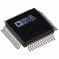
ADV7195KS Analog Devices Inc, ADV7195KS Datasheet - Page 29

ADV7195KS
Manufacturer Part Number
ADV7195KS
Description
IC DAC VID-HDTV 3CH-11BIT 52MQFP
Manufacturer
Analog Devices Inc
Type
Video Encoderr
Datasheet
1.ADV7195KS.pdf
(36 pages)
Specifications of ADV7195KS
Rohs Status
RoHS non-compliant
Applications
HDTV, MPEG, Image Processing
Voltage - Supply, Analog
3.3V
Voltage - Supply, Digital
3.3V
Mounting Type
Surface Mount
Package / Case
52-MQFP, 52-PQFP
Adc/dac Resolution
11b
Screening Level
Commercial
Package Type
MQFP
Pin Count
52
For Use With
EVAL-ADV7195EB - BOARD EVAL FOR ADV7195
Lead Free Status / RoHS Status
Not Compliant
Available stocks
Company
Part Number
Manufacturer
Quantity
Price
Part Number:
ADV7195KSZ
Manufacturer:
ADI/亚德诺
Quantity:
20 000
MODE REGISTER 4
MR4 (MR47–MR40)
(Address (SR4–SR0) = 04H)
Figure 55 shows the various operations under the control of
Mode Register 4.
MR4 BIT DESCRIPTION
Timing Reset (MR40)
Toggling MR40 from low to high and low again resets the inter-
nal horizontal and vertical timing counters.
Reserved (MR41–MR47)
A “0” must be written to these bits.
MODE REGISTER 5
MR5 (MR57–MR50)
(Address (SR4–SR0) = 05H)
Figure 56 shows the various operations under the control of
Mode Register 5.
MR5 BIT DESCRIPTION
Reserved (MR50)
This bit is reserved for the revision code.
RGB Mode (MR51)
When RGB mode is enabled (MR51 = “1”), the ADV7195
accepts unsigned binary RGB data at its input port. This control
is also available in Async Timing Mode.
Sync on PrPb (MR52)
By default the color component output signals Pr, Pb do not con-
tain any horizontal sync pulses. If required, they can be inserted
when MR52 = “1.” This control is not available in RGB Mode.
MR57
MR47
MR56
TO THESE BITS
MR46
BE WRITTEN
MR57–MR54
ZERO MUST
MR55
MR45
ZERO MUST BE
WRITTEN TO
MR47–MR41
THESE BITS
COLOR OUTPUT SWAP
MR53
0
1
MR54
MR44
DAC B = PR
DAC C = R
MR53
Color Output Swap (MR53)
By default DAC B is configured as the Pr output and DAC C as
the Pb output. In setting this bit to “1,” the DAC outputs can
be swapped around so that DAC B outputs Pb and DAC C out-
puts Pr. Table X demonstrates this in more detail.
Reserved (MR54–MR57)
A “0” must be written to these bits.
In 4:4:4 Input Mode
Color Data
Input on Pins
Cr9–0
Cb/Cr9–0
Cr9–0
Cb/Cr9–0
In 4:2:2 Input Mode
Color Data
Input on Pins
Cr9–0
Cb/Cr9–0
Cb/Cr9–0
MR43
Table X. Relationship Between Input Pixel Port, MR53
and DAC B, DAC C Outputs
MR52
0
1
MR52
SYNC ON PrPb
MR42
DISABLE
ENABLE
MR51
MR51
0
1
RGB MODE
MR41
DISABLE
ENABLE
MR40
TIMING RESET
RESERVED FOR
REVISION CODE
MR50
MR53
0
0
1
1
MR53
0 or 1
0
1
MR40
MR50
ADV7195
DAC C (Pb)
DAC C (Pr)
Analog Output
Signal
DAC B
DAC C
DAC C
DAC B
Analog Output
Signal
Not Operational


