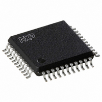
SAA7103H/V4,557 NXP Semiconductors, SAA7103H/V4,557 Datasheet - Page 15

SAA7103H/V4,557
Manufacturer Part Number
SAA7103H/V4,557
Description
IC DIGITAL VIDEO ENCODER 44-QFP
Manufacturer
NXP Semiconductors
Type
Video Encoderr
Datasheet
1.SAA7103HV4557.pdf
(84 pages)
Specifications of SAA7103H/V4,557
Applications
Graphics Controller
Voltage - Supply, Analog
3.15 V ~ 3.45 V
Voltage - Supply, Digital
3 V ~ 3.6 V
Mounting Type
Surface Mount
Package / Case
44-MQFP, 44-PQFP
Lead Free Status / RoHS Status
Lead free / RoHS Compliant
Other names
568-1306
935267649557
SAA7103HB
935267649557
SAA7103HB
Available stocks
Company
Part Number
Manufacturer
Quantity
Price
Company:
Part Number:
SAA7103H/V4,557
Manufacturer:
NXP Semiconductors
Quantity:
10 000
Philips Semiconductors
SAA7102_SAA7103_4
Product data sheet
7.16 I
interlaced, in other cases it may be omitted. If the frame sync signal is present, it is
possible to derive the vertical and the horizontal phase from it by setting the HFS and VFS
bits. HSVGC and VSVGC are not necessary in this case, so it is possible to switch the
pins to output mode.
Alternatively, the device can be triggered by auxiliary codes in a ITU-R BT.656 data
stream via PD7 to PD0.
Only vertical frequencies of 50 Hz and 60 Hz are allowed with the SAA7102; SAA7103. In
Slave mode, it is not possible to lock the encoders color carrier to the line frequency with
the PHRES bits.
In the (more common) Master mode, the time base of the circuit is continuously
free-running. The IC can output a frame sync at pin FSVGC, a vertical sync at pin VSVGC,
a horizontal sync at pin HSVGC and a composite blanking signal at pin CBO. All of these
signals are defined in the PIXCLK domain. The duration of HSVGC and VSVGC are fixed,
they are 64 clocks for HSVGC and 1 line for VSVGC. The leading slopes are in phase and
the polarities can be programmed.
The input line length can be programmed. The field length is always derived from the field
length of the encoder and the pixel clock frequency that is being used.
CBO acts as a data request signal. The circuit accepts input data at a programmable
number of clocks after CBO goes active. This signal is programmable and it is possible to
adjust the following (see
In most cases, the vertical offsets for odd and even fields are equal. If they are not, then
the even field will start later. The SAA7102; SAA7103 will also request the first input lines
in the even field, the total number of requested lines will increase by the difference of the
offsets.
As stated above, the circuit can be programmed to accept the look-up and cursor data in
the first 2 lines of each field. The timing generator provides normal data request pulses for
these lines; the duration is the same as for regular lines. The additional request pulses will
be suppressed with LUTL set to logic 0; see
change in this case, so the first active line can be number 2, counted from 0.
The I
and 400 kbit/s guaranteed transfer rate. It uses 8-bit subaddressing with an
auto-increment function. All registers are write and read, except two read only status
bytes.
The register bit map consists of an RGB Look-Up Table (LUT), a cursor bit map and
control registers. The LUT contains three banks of 256 bytes, where each RGB triplet is
assigned to one address. Thus a write access needs the LUT address and three data
2
•
•
•
•
•
C-bus interface
The horizontal offset
The length of the active part of the line
The distance from active start to first expected data
The vertical offset separately for odd and even fields
The number of lines per input field
2
C-bus interface is a standard slave transceiver, supporting 7-bit slave addresses
Rev. 04 — 18 January 2006
Figure 13
and
Figure
Table
14):
SAA7102; SAA7103
101. The other vertical timings do not
© Koninklijke Philips Electronics N.V. 2006. All rights reserved.
Digital video encoder
15 of 84


