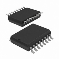
PCA9554D,118 NXP Semiconductors, PCA9554D,118 Datasheet - Page 8

PCA9554D,118
Manufacturer Part Number
PCA9554D,118
Description
IC I/O EXPANDER I2C 8B 16SOIC
Manufacturer
NXP Semiconductors
Specifications of PCA9554D,118
Package / Case
16-SOIC (0.300", 7.5mm Width)
Interface
I²C, SMBus
Number Of I /o
8
Interrupt Output
Yes
Frequency - Clock
400kHz
Voltage - Supply
2.3 V ~ 5.5 V
Operating Temperature
-40°C ~ 85°C
Mounting Type
Surface Mount
Includes
POR
Logic Family
PCA9554
Number Of Lines (input / Output)
8.0 / 8.0
Operating Supply Voltage
2.3 V to 5.5 V
Power Dissipation
200 mW
Operating Temperature Range
- 40 C to + 85 C
Input Voltage
5 V
Logic Type
I2C, SMBus
Maximum Clock Frequency
400 KHz
Mounting Style
SMD/SMT
Number Of Input Lines
8.0
Number Of Output Lines
8.0
Output Current
50 mA
Output Voltage
5 V
Operating Temperature (min)
-40C
Operating Temperature Classification
Industrial
Operating Temperature (max)
85C
Package Type
SO
Rad Hardened
No
Lead Free Status / RoHS Status
Lead free / RoHS Compliant
Lead Free Status / RoHS Status
Lead free / RoHS Compliant, Lead free / RoHS Compliant
Other names
935269192118
PCA9554D-T
PCA9554D-T
PCA9554D-T
PCA9554D-T
Available stocks
Company
Part Number
Manufacturer
Quantity
Price
Part Number:
PCA9554D,118
Manufacturer:
NXP/恩智浦
Quantity:
20 000
NXP Semiconductors
PCA9555_8
Product data sheet
6.2.5 Registers 6 and 7: Configuration registers
6.3 Power-on reset
6.4 I/O port
This register configures the directions of the I/O pins. If a bit in this register is set (written
with ‘1’), the corresponding port pin is enabled as an input with high-impedance output
driver. If a bit in this register is cleared (written with ‘0’), the corresponding port pin is
enabled as an output. Note that there is a high value resistor tied to V
reset, the device's ports are inputs with a pull-up to V
Table 11.
Table 12.
When power is applied to V
condition until V
PCA9555 registers and SMBus state machine will initialize to their default states. The
power-on reset typically completes the reset and enables the part by the time the power
supply is above V
supply, it is necessary to lower it below 0.2 V.
When an I/O is configured as an input, FETs Q1 and Q2 are off, creating a
high-impedance input with a weak pull-up to V
V
If the I/O is configured as an output, then either Q1 or Q2 is on, depending on the state of
the Output Port register. Care should be exercised if an external voltage is applied to an
I/O configured as an output because of the low-impedance path that exists between the
pin and either V
Bit
Symbol
Default
Bit
Symbol
Default
DD
to a maximum of 5.5 V.
Configuration port 0 register
Configuration port 1 register
C0.7
C1.7
7
1
7
1
DD
DD
POR
has reached V
or V
. However, when it is required to reset the part by lowering the power
Rev. 08 — 22 October 2009
C0.6
C1.6
SS
6
1
6
1
.
DD
, an internal power-on reset holds the PCA9555 in a reset
C0.5
C1.5
POR
5
1
5
1
. At that point, the reset condition is released and the
16-bit I
C0.4
C1.4
4
1
4
1
2
DD
C-bus and SMBus I/O port with interrupt
. The input voltage may be raised above
C0.3
C1.3
DD
3
1
3
1
.
C0.2
C1.2
2
2
1
1
DD
PCA9555
© NXP B.V. 2009. All rights reserved.
C0.1
C1.1
at each pin. At
1
1
1
1
C0.0
C1.0
0
1
0
1
8 of 34


