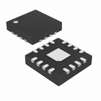
MAX7316ATE+T Maxim Integrated Products, MAX7316ATE+T Datasheet - Page 12

MAX7316ATE+T
Manufacturer Part Number
MAX7316ATE+T
Description
IC I/O EXPANDER I2C 16B 16TQFN
Manufacturer
Maxim Integrated Products
Datasheet
1.MAX7316AEE.pdf
(24 pages)
Specifications of MAX7316ATE+T
Interface
I²C, SMBus
Number Of I /o
10
Interrupt Output
Yes
Frequency - Clock
400kHz
Voltage - Supply
2 V ~ 3.6 V
Operating Temperature
-40°C ~ 125°C
Mounting Type
Surface Mount
Package / Case
16-TQFN Exposed Pad
Lead Free Status / RoHS Status
Lead free / RoHS Compliant
The INT/O8 output pin can be configured as either the
INT output that reflects the interrupt flag logic state or as
a general-purpose output O8. When used as a general-
purpose output, INT/O8 has the same blink and PWM
intensity control capabilities as the other ports.
Set the interrupt enable I bit in the configuration register
to configure INT/O8 as the INT output (Table 4). Clear
interrupt enable to configure INT/O8 as the O8. The O8
logic state is set by the 2 bits O1 and O0 in the configu-
ration register. O8 follows the rules for blinking selected
by the blink enable flag E in the configuration register. If
blinking is disabled, then interrupt output control O0
alone sets the logic state of the INT/O8 pin. If blinking is
enabled, then both interrupt output controls O0 and O1
set the logic state of INT/O8 according to the blink
phase. PWM intensity control for O8 is set by the 4
global intensity bits in the master and O8 intensity reg-
ister (Table 13).
10-Port I/O Expander with LED Intensity
Control, Interrupt, and Hot-Insertion Protection
Table 3. Power-Up Configuration
12
Blink phase 0 outputs P7–P0
Blink phase 1 outputs P7–P0
Ports configuration P7–P0
Outputs Intensity P3, P2
REGISTER FUNCTION
Outputs intensity P1, P0
Outputs intensity P5, P4
Outputs intensity P7, P6
______________________________________________________________________________________
Master, O8 intensity
Configuration
P1, P0 are static logic outputs
P3, P2 are static logic outputs
P5, P4 are static logic outputs
P7, P6 are static logic outputs
PWM oscillator is disabled;
global intensity is enabled
INT/O8 is interrupt output;
POWER-UP CONDITION
High-impedance outputs
High-impedance outputs
O8 is static logic output
Ports P7–P0 are inputs
blink is disabled;
INT/O8 Output
In blink mode, the output ports can be flipped between
using either the blink phase 0 register or the blink
phase 1 register. Flip control is both hardware (the
BLINK input) and software control (the blink flip flag B
in the configuration register) (Table 4).
The blink function can be used for LED effects by pro-
gramming different display patterns in the two sets of
output port registers, and using the software or hard-
ware controls to flip between the patterns.
If the blink phase 1 register is written with 0xFF, then
the BLINK input can be used as a hardware disable to,
for example, instantly turn off an LED pattern pro-
grammed into the blink phase 0 register. This technique
can be further extended by driving the BLINK input with
a PWM signal to modulate the LED current to provide
fading effects.
The blink mode is enabled by setting the blink enable flag
E in the configuration register (Table 4). When blink mode
is enabled, the states of the blink flip flag and the BLINK
input are EXOR’ed to set the phase, and the output ports
are set by either the blink phase 0 register or the blink
phase 1 register (Figure 11) (Table 7).
ADDRESS
CODE
(HEX)
0x01
0x03
0x09
0x0E
0x0F
0x10
0x11
0x12
0x13
D7
1
1
1
0
0
1
1
1
1
D6
1
1
1
0
0
1
1
1
1
D5
1
1
1
0
0
1
1
1
1
REGISTER DATA
D4
1
1
1
0
0
1
1
1
1
D3
1
1
1
1
1
1
1
1
1
D2
Blink Mode
1
1
1
1
1
1
1
1
1
D1
1
1
1
1
0
1
1
1
1
D0
1
1
1
1
0
1
1
1
1


