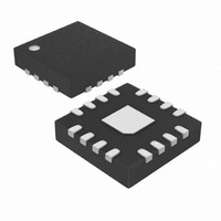
MAX7316ATE+T Maxim Integrated Products, MAX7316ATE+T Datasheet - Page 9

MAX7316ATE+T
Manufacturer Part Number
MAX7316ATE+T
Description
IC I/O EXPANDER I2C 16B 16TQFN
Manufacturer
Maxim Integrated Products
Datasheet
1.MAX7316AEE.pdf
(24 pages)
Specifications of MAX7316ATE+T
Interface
I²C, SMBus
Number Of I /o
10
Interrupt Output
Yes
Frequency - Clock
400kHz
Voltage - Supply
2 V ~ 3.6 V
Operating Temperature
-40°C ~ 125°C
Mounting Type
Surface Mount
Package / Case
16-TQFN Exposed Pad
Lead Free Status / RoHS Status
Lead free / RoHS Compliant
The second (A5), third (A4), fourth (A3), sixth (A1), and
last (A0) bits of the MAX7316 slave address are always
1, 0, 0, 0, and 0. Slave address bits A6 and A2 are
selected by the address input AD0. AD0 can be con-
nected to GND, V+, SDA, or SCL. The MAX7316 has four
possible slave addresses (Table 1), and therefore a
maximum of four MAX7316 devices can be controlled
independently from the same interface.
Table 1. MAX7316 I
Figure 7. Command Byte Received
Figure 8. Command and Single Data Byte Received
Figure 9. n Data Bytes Received
PIN AD0
Control, Interrupt, and Hot-Insertion Protection
GND
SDA
SCL
V+
S
S
HOW COMMAND BYTE AND DATA BYTE MAP INTO
HOW COMMAND BYTE AND DATA BYTE MAP INTO
A6
S
1
1
0
0
ACKNOWLEDGE FROM MAX7316
SLAVE ADDRESS
ACKNOWLEDGE FROM MAX7316
SLAVE ADDRESS
_______________________________________________________________________________________
A5
1
1
1
1
10-Port I/O Expander with LED Intensity
MAX7316'S REGISTERS
MAX7316'S REGISTERS
DEVICE ADDRESS
COMMAND BYTE IS STORED ON RECEIPT OF
A4
2
0
0
0
0
C Slave Address Map
SLAVE ADDRESS
R/W
R/W
A3
ACKNOWLEDGE FROM MAX7316
0
0
0
0
0
0
A2
A
0
1
0
1
A
STOP CONDITION
D15 D14 D13 D12 D11 D10
D15 D14 D13 D12 D11 D10
R/W
A1
0
0
0
0
0
ACKNOWLEDGE FROM MAX7316
COMMAND BYTE
A0
ACKNOWLEDGE FROM MAX7316
COMMAND BYTE
0
0
0
0
A
D15
A write to the MAX7316 comprises the transmission of
the MAX7316’s slave address with the R/W bit set to
zero, followed by at least 1 byte of information. The first
byte of information is the command byte. The com-
mand byte determines which register of the MAX7316
is to be written to by the next byte, if received (Table 2).
If a STOP condition is detected after the command byte
is received, then the MAX7316 takes no further action
beyond storing the command byte.
Any bytes received after the command byte are data
bytes. The first data byte goes into the internal register
of the MAX7316 selected by the command byte (Figure
8). If multiple data bytes are transmitted before a STOP
condition is detected, these bytes are generally stored
in subsequent MAX7316 internal registers because the
command byte address autoincrements (Table 2). A
diagram of a write to the output ports registers (blink
phase 0 register or blink phase 1 register) is given in
Figure 10.
D14
D9
D9
D13
D8
D8
COMMAND BYTE
Message Format for Writing the MAX7316
D12
A
A
ACKNOWLEDGE FROM MAX7316
D7
D7
D11
AUTOINCREMENT MEMORY ADDRESS
AUTOINCREMENT MEMORY ADDRESS
D6
D6
D10
D5
D5
ACKNOWLEDGE FROM MAX7316
ACKNOWLEDGE FROM MAX7316
DATA BYTE
D9
D4
DATA BYTE
D4
BYTE
BYTES
1
N
D3
D8
D3
D2
D2
A
D1
D1
P
D0
D0
A
A
P
P
9


