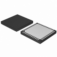
AMIS49587C5872RG ON Semiconductor, AMIS49587C5872RG Datasheet - Page 20

AMIS49587C5872RG
Manufacturer Part Number
AMIS49587C5872RG
Description
IC MODEM PLC 50/60MHZ 52QFN
Manufacturer
ON Semiconductor
Datasheet
1.AMIS49587C5871RG.pdf
(55 pages)
Specifications of AMIS49587C5872RG
Baud Rates
Selectable
Interface
SCI
Voltage - Supply
3 V ~ 3.6 V
Mounting Type
Surface Mount
Package / Case
52-TQFN Exposed Pad
Lead Free Status / RoHS Status
Lead free / RoHS Compliant
Data Format
-
Available stocks
Company
Part Number
Manufacturer
Quantity
Price
Company:
Part Number:
AMIS49587C5872RG
Manufacturer:
Seagate
Quantity:
1 000
mains and CHIP_CLK can be tuned. This opens the
possibility to compensate for external delay t
coupler) and for the 1.9 V positive threshold VIR
of the zero crossing detector. This is done by pre- -loading the
PLL counter with a number value stored in register
R_ZC_ADJUST[7:0]. The adjustment period or granularity
is 26 ms. The maximum adjustment is 255 x 26 ms = 6.6 ms
which corresponds with 1/3rd of the mains sine period.
6.1.3 Oscillator
crystal of 24 MHz. XIN is the input to the oscillator inverter
gain stage and XOUT is the output.
*The start of the Physical Subframe is shifted back with R_ZC_ADJUST[7:0] x 26 mS = t
Table 23. ZERO CROSS DELAY COMPENSATION
The phase difference between the zero crossing of the
The oscillator works with a standard parallel resonance
R_ZC_ADJUST[7:0]
0000 0000
0000 0001
0000 0010
0000 0011
1111 1101
1111 1110
1111 1111
…
Figure 14. Zero Cross Adjustment to Compensate for Zero Cross Delay (Example for 50 Hz)
CHIP _CLK
ZeroCross
VIR
V
M 50HZIN
MAINS
Compensation
Start of Physical PreFrame*
6589 ms
6615 ms
6641 ms
26 ms
52 ms
78 ms
0 ms
…
PLL in lock
t
ZCD
ZCD
(e.g. opto
M50HZIN
http://onsemi.com
10 ms
20
Figure 15 must be connected to the oscillator pins. For a
crystal requiring a parallel capacitance of 20 pF C
around 30 pF. (Values of capacitors are indicative only and
are given by the crystal manufacturer). To guarantee startup
the series loss resistance of the crystal must be smaller than
80 Ω. A parallel resistor R
improve the clock symmetry.
frequency for the complete IC. The clock frequency for the
ARM f
is equal to f
clock signals will be derived from f
the receiver, f
receiver internal clock signals will be derived from
f
RX_CLK
Figure 15. Placement of the Capacitors and Crystal
For correct functionality the external circuit illustrated in
The oscillator output f
XTAL _IN
C
ARM
X
with Clock Signal Generated Internally
.
CLK
= f
ZCD
RX_CLK
CLK.
/ 2 or 12 MHz. All the transmitter internal
to compensate for the zero cross delay
The clock for the transmitter, f
6 bit @ 300 baud
is equal to f
24 MHz
R
V
X
CLK
SSA
X
= 1 MΩ is recommended to
= 24 MHz is the base
CLK
t
XTAL _ OUT
C
TX_CLK
X
/ 4 or 6 MHz. All the
. The clock for
X
must be
TX_CLK


