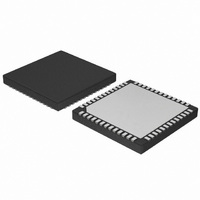
AMIS49587C5872RG ON Semiconductor, AMIS49587C5872RG Datasheet - Page 7

AMIS49587C5872RG
Manufacturer Part Number
AMIS49587C5872RG
Description
IC MODEM PLC 50/60MHZ 52QFN
Manufacturer
ON Semiconductor
Datasheet
1.AMIS49587C5871RG.pdf
(55 pages)
Specifications of AMIS49587C5872RG
Baud Rates
Selectable
Interface
SCI
Voltage - Supply
3 V ~ 3.6 V
Mounting Type
Surface Mount
Package / Case
52-TQFN Exposed Pad
Lead Free Status / RoHS Status
Lead free / RoHS Compliant
Data Format
-
Available stocks
Company
Part Number
Manufacturer
Quantity
Price
Company:
Part Number:
AMIS49587C5872RG
Manufacturer:
Seagate
Quantity:
1 000
3.3
VDDA
VDDA is the positive analog supply pin. Nominal voltage is 3.3 V. A ceramic decoupling capacitor C
be placed between this pin and the VSSA. Connection path of this capacitance to the VSSA on the PCB should be kept as short
as possible in order to minimize the serial resistance.
REF_OUT
REF_OUT is the analog output pin which provides the voltage reference used by the A/D converter. This pin must be
decoupled to the analog ground by a 1 mF ±10 percent ceramic capacitance C
the VSSA on the PCB should be kept as short as possible in order to minimize the serial resistance.
VSSA
VSSA is the analog ground supply pin.
VDD
VDD is the 3.3 V digital supply pin. A ceramic decoupling capacitor C
and the VSS. Connection path of this capacitance to the VSS on the PCB should be kept as short as possible in order to minimize
the serial resistance.
VSS
VSS is the digital ground supply pin.
Table 7. AMIS- -49587 QFN PIN FUNCTION DESCRIPTION
2, 3, ..
50, 52
P:
A:
D:
No.
Pin
37
42
43
46
47
48
49
51
Detailed Pin Description
Power pin
Analog pin
Digital pin
Pin Name
REF_OUT
RX_OUT
TX_ENB
TX_OUT
ALC_IN
RX_IN
VDDA
VSSA
NC
Out
Out
Out
Out
I/O
In
In
D, 5V Safe
5V Safe: IO that support the presence of 5 V on bus line
Out:
In:
Type
A
A
P
P
A
A
A
http://onsemi.com
Output signal
Input signal
TX enable bar (open drain)
Transmitter output
Automatic level control input
3.3 V analog supply
Analog ground
Output of receiver low noise operational amplifier
Positive input of receiver low noise operational amplifier
Reference output for stabilization
Pins 2, 3, 4, 5, 12, 13, 14, 15, 19,23, 25, 26, 27, 28, 30, 34, 38, 39, 40,
42, 44, 45, 50, 52 are not connected. These pins need to be left open or
connected to the GND plane
7
DD
= 100 nF ±10% must be placed between this pin
DREF
. The connection path of this capacitor to
Description
DA
= 100 nF ±10% must


