SCAN12100TYA/NOPB National Semiconductor, SCAN12100TYA/NOPB Datasheet - Page 11
SCAN12100TYA/NOPB
Manufacturer Part Number
SCAN12100TYA/NOPB
Description
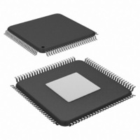
IC SERIAL/DESERIAL CPRI 100-TQFP
Manufacturer
National Semiconductor
Series
SCANr
Datasheet
1.SCAN12100TYANOPB.pdf
(34 pages)
Specifications of SCAN12100TYA/NOPB
Function
Serializer/Deserializer
Data Rate
614.4Mbps
Input Type
LVTTL/LVCMOS
Output Type
LVTTL, LVCMOS
Number Of Inputs
10
Number Of Outputs
10
Voltage - Supply
1.8 V ~ 3.3 V
Operating Temperature
-40°C ~ 85°C
Mounting Type
Surface Mount
Package / Case
100-TQFP Exposed Pad, 100-eTQFP, 100-HTQFP, 100-VQFP
Lead Free Status / RoHS Status
Lead free / RoHS Compliant
Other names
SCAN12100TYA
Available stocks
Company
Part Number
Manufacturer
Quantity
Price
Company:

Part Number:
SCAN12100TYA/NOPB
Manufacturer:
Texas Instruments
Quantity:
10 000


Note 1: “Absolute Maximum Ratings” are the ratings beyond which the safety of the device cannot be guaranteed. They are not meant to imply that the device
should be operated at these limits.
Note 2: Typical parameters are measured at nominal supply levels and T
= 25°C. They are for reference purposes and are not production-tested.
A
Note 3: Transmit Jitter testing methodology is defined in Appendix 48B of IEEE 802.2ae-2002. The SCAN12100 transmit output jitter is constant for all valid CPRI
datarates. The transmit jitter is significantly less than the specified limits in terms of UI.
Note 4: CJPAT is a stress pattern defined in IEEE 802.2ae-2002 Appendix 48A
Note 5: CDET nominal valid duration is determined by the CPRI data rate. CDET timing is similar to the ROUT[0:9] timing.
Note 6: Transmit or Receive K28.5 pattern. Assumes TXCLK is stable and toggles only after all SerDes clocks become synchronous.
Note 7: Conditions: The TX PLL is locked, the TXCLK is stable and the TXCLK is synchronous.
Note 8: Transmit latency is fixed once the link is established and is guaranteed by the Tser specification.
Note 9: Receive latency is fixed once the link is established and is guaranteed by the Tdes specification.
Note 10: Receiver output timing specifications for TS-R and TH-R are tested at the CPRI rate of 1.2288 Gbps.
Note 11: Limits are guaranteed by design and characterization over process, supply voltage, and temperature variations.
Note 12: Limits are guaranteed by design.
Note 13: Serial side DCM readings are referenced to the first bit of the K28.5 pattern {110000 0101 001111 1010}. Parallel side DCM readings are referenced
to the TXCLK or RXCLK edge (not the data edge) that registers the K character as an input or output.
Note 14: DCM readings are valid when the RXCLK pin on the SCAN12100 is used as an output in "WRITE" mode (RXCLKMODE = 0) and IOVDD = 3.3V.
Note 15: Edge rate characterization includes the loading effects of 1.0 uF AC-coupling capacitors and 4 inches of 100 ohm differential microstrip.
11
www.national.com
Related parts for SCAN12100TYA/NOPB
Image
Part Number
Description
Manufacturer
Datasheet
Request
R

Part Number:
Description:
National Semiconductor [8-Bit D/A Converter]
Manufacturer:
National Semiconductor
Datasheet:
Part Number:
Description:
National Semiconductor [Media Coprocessor]
Manufacturer:
National Semiconductor
Datasheet:
Part Number:
Description:
Digitally Controlled Tone and Volume Circuit with Stereo Audio Power Amplifier, Microphone Preamp Stage and National 3D Sound
Manufacturer:
National Semiconductor
Datasheet:
Part Number:
Description:
Digitally Controlled Tone and Volume Circuit with Stereo Audio Power Amplifier, Microphone Preamp Stage and National 3D Sound
Manufacturer:
National Semiconductor
Datasheet:
Part Number:
Description:
AC97 Rev 2 Codec with Sample Rate Conversion and National 3D Sound
Manufacturer:
National Semiconductor
Part Number:
Description:
Manufacturer:
National Semiconductor
Datasheet:
Part Number:
Description:
Manufacturer:
National Semiconductor
Datasheet:
Part Number:
Description:
General Purpose, Low Voltage, Low Power, Rail-to-Rail Output Operational Amplifiers
Manufacturer:
National Semiconductor
Datasheet:
Part Number:
Description:
8-bit 20 MSPS flash A/D converter.
Manufacturer:
National Semiconductor
Datasheet:
Part Number:
Description:
Low Noise Quad Operational Amplifier
Manufacturer:
National Semiconductor
Datasheet:
Part Number:
Description:
Quad Differential Line Receivers
Manufacturer:
National Semiconductor
Datasheet:
Part Number:
Description:
Quad High Speed Trapezoidal? Bus Transceiver
Manufacturer:
National Semiconductor
Datasheet:
Part Number:
Description:
Dual Line Receiver
Manufacturer:
National Semiconductor
Datasheet:
Part Number:
Description:
TTL to 10k ECL Level Translator with Latch
Manufacturer:
National Semiconductor
Datasheet: