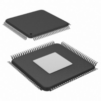
SCAN12100TYA/NOPB National Semiconductor, SCAN12100TYA/NOPB Datasheet - Page 7

SCAN12100TYA/NOPB
Manufacturer Part Number
SCAN12100TYA/NOPB
Description
IC SERIAL/DESERIAL CPRI 100-TQFP
Manufacturer
National Semiconductor
Series
SCANr
Datasheet
1.SCAN12100TYANOPB.pdf
(34 pages)
Specifications of SCAN12100TYA/NOPB
Function
Serializer/Deserializer
Data Rate
614.4Mbps
Input Type
LVTTL/LVCMOS
Output Type
LVTTL, LVCMOS
Number Of Inputs
10
Number Of Outputs
10
Voltage - Supply
1.8 V ~ 3.3 V
Operating Temperature
-40°C ~ 85°C
Mounting Type
Surface Mount
Package / Case
100-TQFP Exposed Pad, 100-eTQFP, 100-HTQFP, 100-VQFP
Lead Free Status / RoHS Status
Lead free / RoHS Compliant
Other names
SCAN12100TYA
Available stocks
Company
Part Number
Manufacturer
Quantity
Price
Company:
Part Number:
SCAN12100TYA/NOPB
Manufacturer:
Texas Instruments
Quantity:
10 000
LVCMOS DC SPECIFICATIONS (1.8V I/O)
V
V
I
V
V
I
C
LVCMOS DC SPECIFICATIONS (3.3V I/O)
V
V
I
V
V
I
C
JTAG DC SPECIFICATIONS (3.3V I/O)
V
V
I
V
IN
OZ
IN
OZ
IN
IH
IL
OH
OL
IH
IL
OH
OL
IH
IL
OH
IO
IO
Symbol
Absolute Maximum Ratings
If Military/Aerospace specified devices are required,
please contact the National Semiconductor Sales Office/
Distributors for availability and specifications.
Electrical Characteristics
Supply Voltage (AV
Supply Voltage (PV
Supply Voltage (AV
LVCMOS Input Voltage
LVCMOS Output Voltage
MDC/MDIO/ADD[0:4],VSEL Input Voltage
MDIO Output Voltage
CML Receiver Input Voltage
CML Receiver Output Voltage
Junction Temperature
Storage Temperature
Lead Temperature
Maximum Package Power Dissipation at 25°C
Note: This is the maximum TQFP-100 package power
dissipation capability. For SCAN12100 power dissipation,
see the information in the Electrical Characteristics section.
Soldering, 10–20 sec
Lead-free +260°C flow is available
100-pin TQFP with Exposed Pad
High level input voltage
Low level input voltage
Input Current
High level output voltage
Low level output voltage
Power Down Output Current
Input/Output Capacitance
High level input voltage
Low level input voltage
Input Current
High level output voltage
Low level output voltage
Power Down Output Current
Input/Output Capacitance
High level input voltage
Low level input voltage
Input Current
High level output voltage
DD18
DD
DD33
, IOV
Parameter
)
)
DD
)
−0.3V to (AV
−0.3V to (AV
−0.3V to (IOV
−0.3V to (IOV
−0.3V to (AV
−0.3V to (AV
−65°C to +150°C
−0.3V to +2.0V
−0.3V to +3.6V
−0.3V to +3.6V
Over recommended operating supply and temperature ranges unless other specified.
DD33
V
I
I
Power down
Typical
V
I
I
Power down
Typical
V
I
(Note 1)
OH
OL
OH
OL
OH
IN
IN
IN
= 2 mA
= 2 mA
= −2 mA
= −2 mA
= −2 mA
= 0V or 1.9V
= 0V or 3.465V
= 0V or 3.465V
+125°C
+ 0.5V)
4.16 W
235 °C
DD33
0.5V)
0.5V)
0.5V)
0.3V)
0.3V)
DD
DD
DD
DD
+
+
+
+
+
Condition
7
Supply Voltage
AV
AV
IOV
IOV
Temperature
Junction temperature
Supply Noise
Recommended Operating
Conditions
Derating above 25°C
Thermal Resistance , θ
ESD Rating
CML RIN/DOUT Pins
All Other Pins
(Peak-to-Peak)
HBM, 1.5 kΩ, 100 pF
EIAJ, 0Ω, 200 pF
CDM
HBM, 1.5 kΩ, 100 pF
EIAJ, 0Ω, 200 pF
CDM
DD18
DD33
DD
DD
(1.8V Mode)
(3.3V Mode)
, PV
DD33
0.65V
Min
−10
−20
−10
−20
−35
1.2
2.4
2.4
2
2
DD
JA
(0 airflow)
(Note 2)
3.135
3.135
Typ
2.8
2.8
Min
1.7
1.7
-40
Typ
1.8
3.3
1.8
3.3
25
0.35V
Max
0.45
+50
+20
+50
+20
+50
0.8
0.4
0.8
3.465
3.465
<100
DD
Max
41.6 mW/°C
125
1.9
1.9
85
www.national.com
24.0°C/W
>250V
>250V
>8 kV
>2 kV
>7 kV
>2 kV
Units
Unit
mV
°C
°C
µA
µA
pF
µA
µA
pF
µA
V
V
V
V
V
V
V
V
V
V
V
V
V
V
V


