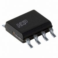
PCA9600D,118 NXP Semiconductors, PCA9600D,118 Datasheet - Page 9

PCA9600D,118
Manufacturer Part Number
PCA9600D,118
Description
IC DUAL BI-DIR BUS BUFFER 8-SOIC
Manufacturer
NXP Semiconductors
Type
Bufferr
Datasheet
1.PCA9600DP118.pdf
(30 pages)
Specifications of PCA9600D,118
Package / Case
8-SOIC (3.9mm Width)
Tx/rx Type
I²C Logic
Delay Time
100ns
Capacitance - Input
10pF
Voltage - Supply
2.5 V ~ 15 V
Current - Supply
7.3mA
Mounting Type
Surface Mount
Logic Family
SDA, SCL
Supply Voltage (max)
15 V
Supply Voltage (min)
2 V
Maximum Operating Temperature
+ 85 C
Mounting Style
SMD/SMT
Interface
I2C Bus
Maximum Power Dissipation
300 mW
Minimum Operating Temperature
- 40 C
Output Current
2 mA
Output Voltage
15 V
Supply Current
5.5 mA
Logic Type
Bidirectional Bus Buffer
Lead Free Status / RoHS Status
Lead free / RoHS Compliant
For Use With
568-4704 - DAUGHTER CARD PCA9600 FOR OM6275
Lead Free Status / Rohs Status
Lead free / RoHS Compliant
Other names
935285243118
PCA9600D-T
PCA9600D-T
PCA9600D-T
PCA9600D-T
NXP Semiconductors
Table 6.
T
unless otherwise specified. Typical values are measured at V
[1]
[2]
[3]
[4]
[5]
PCA9600_4
Product data sheet
Symbol Parameter
Buffer response time
V
t
Input capacitance
C
d
amb
CC
i
The maximum static sink current for a standard I
holding the bus LOW. However, when an external device pulls the SX/SY pins below 1.4 V, the PCA9600 may source a current between
0 mA and 1 mA maximum. During contention an external device is required to pull the bus connected to SX or SY down to the 0.4 V
level referenced in the I
Therefore the external pull-up used at SX/SY should be limited to 2 mA. The typical and maximum currents sourced by SX/SY as a
function of junction temperature are shown in
Valid over temperature for V
The input logic threshold is independent of the supply voltage.
The minimum value requirement for pull-up current, 0.3 mA, guarantees that the minimum value for V
the maximum V
IC. While the tolerances on absolute levels allow a small probability, the LOW from one SX output is recognized by an SX input of
another PCA9600, this has no consequences for normal applications. In any design the SX pins of different ICs should never be linked
because the resulting system would be very susceptible to induced noise and would not support all I
The fall time of V
The fall time of V
The rise time of V
The rise time of V
= 5 V; pin TX pull-up resistor = 160 ; pin SX pull-up resistor = 2.2 k ; no capacitive load
= 40 C to +85 C unless otherwise specified; voltages are specified with respect to GND with V
delay time
input capacitance
Characteristics
SX
TX
SX
TX
SX
input HIGH level to eliminate any possibility of latching. The specified difference is guaranteed by design within any
from 5 V to 2.5 V in the test is approximately 10 ns.
from 5 V to 2.5 V in the test is approximately 20 ns.
from 0 V to 2.5 V in the test is approximately 15 ns.
from 0.7 V to 2.5 V in the test is approximately 25 ns.
[5]
2
C-bus specification. So that device must be able to sink up to 1 mA from SX/SY plus the usual pull-up current.
…continued
CC
5 V. At higher V
Figure
2
CC
C-bus is 3 mA and PCA9600 is guaranteed to sink 3 mA at SX/SY when those pins are
Rev. 04 — 11 November 2009
Conditions
V
falling input between
V
threshold, and V
falling to 50 % V
V
rising input between
V
threshold, and V
reaching 50 % V
V
falling input between
V
threshold, and V
falling to 50 % V
V
rising input between
V
threshold, and V
reaching 50 % V
effective input capacitance of
any signal pin measured by
incremental bus rise times;
guaranteed by design, not
production tested
, this current may increase to maximum 20 A at V
SX
SX
SX
SX
RX
RX
RX
RX
10, and the equivalent circuit at the SX/SY interface is shown in
to V
= input switching
to V
= input switching
to V
= input switching
to V
= input switching
TX
TX
SX
SX
, V
, V
, V
, V
CC
SY
SY
RY
RY
= 5 V and T
to V
CC
to V
CC
to V
to V
TX
TX
SX
SX
CC
CC
output
output
output
output
TY
TY
SY
SY
; on
; on
; on
; on
amb
= 25 C.
Min
-
-
-
-
-
Dual bidirectional bus buffer
2
SX
C-bus operating modes.
CC
output LOW will always exceed
Typ
50
60
100
95
-
= 15 V.
CC
PCA9600
© NXP B.V. 2009. All rights reserved.
= 2.5 V to 15 V
Max
-
-
-
-
10
Figure
4.
9 of 30
Unit
ns
ns
ns
ns
pF


