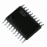
PCA9518APW,512 NXP Semiconductors, PCA9518APW,512 Datasheet - Page 14

PCA9518APW,512
Manufacturer Part Number
PCA9518APW,512
Description
IC I2C HUB 5CH EXPANDBL 20-TSSOP
Manufacturer
NXP Semiconductors
Datasheet
1.PCA9518APW512.pdf
(23 pages)
Specifications of PCA9518APW,512
Applications
CMOS Bus Controller
Interface
I²C
Voltage - Supply
3 V ~ 3.6 V
Package / Case
20-TSSOP
Mounting Type
Surface Mount
Lead Free Status / RoHS Status
Lead free / RoHS Compliant
Other names
568-4245-5
935284254512
PCA9518APW
935284254512
PCA9518APW
NXP Semiconductors
Table 7.
V
[1]
[2]
[3]
[4]
PCA9518A_3
Product data sheet
Symbol
t
t
t
t
t
t
t
t
t
PHL
PLH
PHL1
PLH1
PLH2
THL
TLH
su
h
DD
= 2.3 V to 2.7 V
For operation between published voltage ranges, refer to worst-case parameter in both ranges.
The SDA and SCL propagation delays are dominated by rise times or fall times. The fall times are mostly internally controlled and are
only sensitive to load capacitance. The rise times are RC time constant controlled and therefor a specific numerical value can only be
given for fixed RC time constants.
The SDA HIGH to LOW propagation delay includes the fall time from V
SCL fall time from the quiescent HIGH (usually V
included which make the fall time almost independent of load capacitance.
The SDA or SCL LOW to HIGH propagation delay includes the rise time constant from the quiescent LOW to 0.5V
or EXPSCL2, the rise time constant for the quiescent LOW to 0.5V
the quiescent external driven LOW to 0.7V
external resistance and total capacitance for the various nodes.
Parameter
HIGH to LOW propagation delay
LOW to HIGH propagation delay
HIGH to LOW propagation delay 1
LOW to HIGH propagation delay 1
LOW to HIGH propagation delay 2
HIGH to LOW output transition time
LOW to HIGH output transition time
set-up time
hold time
Dynamic characteristics
[1]
; V
SS
Fig 7.
= 0 V; T
amb
AC waveforms
EXPSDA1 or EXPSCL1
EXPSDA2 or EXPSCL2
= 40 C to +85 C; unless otherwise specified.
DD
output SDA or SCL
input SDA or SCL
for the SDA or SCL output. All of these rise times are RC time constants determined by the
DD
Rev. 03 — 3 December 2008
) to below 0.3V
Conditions
SDA to SDAn, or
SCL to SCLn;
SDA to SDAn, or
SCL to SCLn;
EXPSDA1 to SDA, or
EXPSCL1 to SCL;
EXPSDA1 to SDA, or
EXPSCL1 to SCL;
EXPSDA2 to SDA, or
EXPSCL2 to SCL;
SDA, SCL;
SDA, SCL;
enable to START condition
enable after STOP condition
0.7V
t
PHL1
Figure 7
Figure 7
t
PHL2
DD
DD
DD
0.5V
Figure 7
Figure 7
. The SDA and SCL outputs have edge rate control circuits
t
t
for the EXPSDA1 or EXPSCL1, and the rise time constant from
PHL
PHL1
0.7V
DD
DD
0.52 V
Figure 7
Figure 7
Figure 7
to 0.5V
DD
0.3V
t
THL
0.4 V
0.5V
DD
DD
DD
t
THL
of the EXPSDA1 or EXPSCL1 pins and the SDA or
0.3V
effective
stretch
DD
Expandable 5-channel I
[2][3]
[2][4]
0.4 V
t
PLH2
0.5V
0.3V
0.5V
Min
105
110
109
130
160
58
-
300
300
DD
0.3V
DD
DD
t
DD
TLH
t
TLH
Typ
202
259
193
153
234
110
0.85 RC
-
-
PCA9518A
0.7V
t
t
002aac533
PLH1
PLH2
0.7V
© NXP B.V. 2008. All rights reserved.
DD
t
DD
PLH
DD
for the EXPSDA1
Max
389
265
327
179
279
187
-
-
-
2
C-bus hub
14 of 23
Unit
ns
ns
ns
ns
ns
ns
ns
ns
ns


