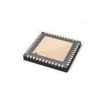
PTN3360DBS,518 NXP Semiconductors, PTN3360DBS,518 Datasheet - Page 9

PTN3360DBS,518
Manufacturer Part Number
PTN3360DBS,518
Description
IC DVI/HDMI LVL SHIFTER 48HVQFN
Manufacturer
NXP Semiconductors
Type
Level Shifterr
Datasheet
1.PTN3360DBS518.pdf
(25 pages)
Specifications of PTN3360DBS,518
Package / Case
48-VFQFN Exposed Pad
Applications
DisplayPort to HDMI, DVI Adapters
Interface
DVI, HDMI
Voltage - Supply
2.85 V ~ 3.6 V
Mounting Type
Surface Mount
Maximum Operating Temperature
+ 85 C
Minimum Operating Temperature
- 40 C
Mounting Style
SMD/SMT
Lead Free Status / RoHS Status
Lead free / RoHS Compliant
Lead Free Status / RoHS Status
Lead free / RoHS Compliant, Lead free / RoHS Compliant
Other names
568-5120-2
Available stocks
Company
Part Number
Manufacturer
Quantity
Price
Company:
Part Number:
PTN3360DBS,518
Manufacturer:
LT
Quantity:
89
NXP Semiconductors
PTN3360D
Product data sheet
Table 3.
Symbol
OUT_D2−
OUT_D1−
SCL_SOURCE 9
SDA_SOURCE 8
SCL_SINK
SDA_SINK
DDC_EN
Supply and ground
V
GND
OUT_D1+
HPD and DDC signals
HPD_SINK
HPD_SOURCE 7
DD
[1]
Pin description
All information provided in this document is subject to legal disclaimers.
Pin
20
22
23
30
28
29
32
2, 11,
15, 21,
26, 33,
40, 46
1, 5,
12, 18,
24, 27,
31, 36,
37, 43
Rev. 2 — 19 November 2010
TMDS differential
TMDS differential
single-ended 3.3 V
single-ended 3.3 V
single-ended 5 V
single-ended 5 V
3.3 V CMOS input
Type
output
TMDS differential
output
output
5 V CMOS
single-ended input
3.3 V CMOS
single-ended output
open-drain DDC I/O
open-drain DDC I/O
open-drain DDC I/O
open-drain DDC I/O
3.3 V DC supply
ground
…continued
HDMI/DVI level shifter supporting deep color mode
Description
HDMI compliant TMDS output. OUT_D2− makes
a differential pair with OUT_D2+. OUT_D2− is in
phase with IN_D2−.
HDMI compliant TMDS output. OUT_D1+ makes
a differential pair with OUT_D1−. OUT_D1+ is in
phase with IN_D1+.
HDMI compliant TMDS output. OUT_D1− makes
a differential pair with OUT_D1+. OUT_D1− is in
phase with IN_D1−.
0 V to 5 V (nominal) input signal. This signal
comes from the DVI or HDMI sink. A HIGH value
indicates that the sink is connected; a LOW value
indicates that the sink is disconnected.
HPD_SINK is pulled down by an integrated
200 kΩ pull-down resistor.
0 V to 3.3 V (nominal) output signal. This is
level-shifted version of the HPD_SINK signal.
3.3 V source-side DDC clock I/O. Pulled up by
external termination to 3.3 V. 5 V tolerant I/O.
3.3 V source-side DDC data I/O. Pulled up by
external termination to 3.3 V. 5 V tolerant I/O.
5 V sink-side DDC clock I/O. Pulled up by
external termination to 5 V. Provides rise time
acceleration for LOW-to-HIGH transitions.
5 V sink-side DDC data I/O. Pulled up by
external termination to 5 V. Provides rise time
acceleration for LOW-to-HIGH transitions.
Enables the DDC buffer and level shifter.
When DDC_EN = LOW, buffer/level shifter is
disabled.
When DDC_EN = HIGH, buffer and level shifter
are enabled.
Supply voltage; 3.3 V ± 10 %.
Supply ground. All GND pins must be connected
to ground for proper operation.
PTN3360D
© NXP B.V. 2010. All rights reserved.
9 of 25


