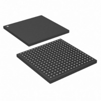
DS33X41+ Maxim Integrated Products, DS33X41+ Datasheet - Page 22

DS33X41+
Manufacturer Part Number
DS33X41+
Description
IC MAPPING ETHERNET 256CSBGA
Manufacturer
Maxim Integrated Products
Datasheet
1.DS33X11.pdf
(375 pages)
Specifications of DS33X41+
Applications
Data Transport
Interface
Parallel/Serial
Voltage - Supply
1.8V, 2.5V, 3.3V
Package / Case
256-CSBGA
Mounting Type
Surface Mount
Lead Free Status / RoHS Status
Lead free / RoHS Compliant
- Current page: 22 of 375
- Download datasheet (3Mb)
Rev: 063008
________________________________________________ DS33X162/X161/X82/X81/X42/X41/X11/W41/W11
SPI_SWAP
SPI_CPHA
SPI_CPOL
SPI_SEL
WR/RW
RD/DS
MODE
NAME
ALE
D5/
D6/
D7/
INT
CS
PACKAGE PINS
256
J10
J12
J11
J16
M9
L8
K9
J8
J9
J7
144
G5
K5
J5
L5
J3
—
—
—
—
—
TYPE
IOz
IOz
IOz
Oz
I
I
I
I
I
I
Data Bit 5. Bi-directional data bit 5 of the microprocessor interface. Not
driven when CS=1 or RST=0.
SPI_SWAP (SPI_SEL=1). Controls the address and data bit order of the
SPI interface. The R/W and B bit positions do not change.
0 = LSB is transmitted and received first. The resulting bit order is:
1 = MSB is transmitted and received first. The resulting bit order is:
Data Bit 6. Bi-directional data bit 6 of the microprocessor interface. Not
driven when CS=1 or RST=0.
SPI_CPHA (SPI_SEL=1). When in SPI mode, setting this bit to 1 inverts
the phase of the clock signal on SPICK. See Section 2.10 for detailed
timing and functionality information. Default setting is low.
Data Bit 7. Bi-directional data bit 7 of the microprocessor interface. Not
driven when CS=1 or RST=0.
SPI_CPOL (SPI_SEL=1). When in SPI mode, setting this bit to 1 inverts
the clock signal on SPICK. See Section 2.10 for detailed timing and
functionality information. Default setting is low.
Chip Select. This pin must be taken low for read/write operations. When
CS is high, the RD/DS and WR signals are ignored.
Read Data Strobe (Intel Mode). The device drives the data bus with the
contents of the addressed register while RD and CS are both low.
Data Strobe (Motorola Mode). Used to latch data through the
microprocessor interface. DS must be low during read and write
operations.
Write (Intel Mode). The device captures the contents of the data bus on
the rising edge of WR and writes them to the addressed register location.
CS must be held low during write operations.
Read Write (Motorola Mode). Used to indicate read or write operation.
RW must be set high for a register read cycle and low for a register write
cycle.
Address Latch Enable. This signal is used to internally latch an address,
allowing multiplexing of the parallel interface address and data lines.
When ALE is high, the values of the A[10:0] pins are used for read/write
operations. On the falling edge of ALE, the values of the A[10:0] pins are
latched internally, and the latched value is used for read/write operations
until the next rising edge of ALE. ALE should be tied high for non-
multiplexed address systems.
Mode. Selects RD/WR or DS strobe mode.
0 = Read/Write Strobe Mode
1 = Data Strobe Mode
Interrupt Output. Outputs a logic zero when an unmasked interrupt event
is detected. INT is de-asserted when all interrupts have been
acknowledged and serviced. Active low. Inactive state is configured with
the GL.CR2.INTM bit.
Parallel/SPI Interface Select
0 = Parallel Interface
1 = SPI Interface Selected
R/W, A7, A8, A9, A10, A11, A12, A13,
A0, A1, A2, A3, A4, A5, A6, Burst,
D0, D1, D2, D3, D4, D5, D6, D7...
R/W, A13, A12, A11, A10, A9, A8, A7,
A6, A5, A4, A3, A2, A1, A0, Burst,
D7, D6, D5, D4, D3, D2, D1, D0…
FUNCTION
22 of 375
Related parts for DS33X41+
Image
Part Number
Description
Manufacturer
Datasheet
Request
R

Part Number:
Description:
MAX7528KCWPMaxim Integrated Products [CMOS Dual 8-Bit Buffered Multiplying DACs]
Manufacturer:
Maxim Integrated Products
Datasheet:

Part Number:
Description:
Single +5V, fully integrated, 1.25Gbps laser diode driver.
Manufacturer:
Maxim Integrated Products
Datasheet:

Part Number:
Description:
Single +5V, fully integrated, 155Mbps laser diode driver.
Manufacturer:
Maxim Integrated Products
Datasheet:

Part Number:
Description:
VRD11/VRD10, K8 Rev F 2/3/4-Phase PWM Controllers with Integrated Dual MOSFET Drivers
Manufacturer:
Maxim Integrated Products
Datasheet:

Part Number:
Description:
Highly Integrated Level 2 SMBus Battery Chargers
Manufacturer:
Maxim Integrated Products
Datasheet:

Part Number:
Description:
Current Monitor and Accumulator with Integrated Sense Resistor; ; Temperature Range: -40°C to +85°C
Manufacturer:
Maxim Integrated Products

Part Number:
Description:
TSSOP 14/A�/RS-485 Transceivers with Integrated 100O/120O Termination Resis
Manufacturer:
Maxim Integrated Products

Part Number:
Description:
TSSOP 14/A�/RS-485 Transceivers with Integrated 100O/120O Termination Resis
Manufacturer:
Maxim Integrated Products

Part Number:
Description:
QFN 16/A�/AC-DC and DC-DC Peak-Current-Mode Converters with Integrated Step
Manufacturer:
Maxim Integrated Products

Part Number:
Description:
TDFN/A/65V, 1A, 600KHZ, SYNCHRONOUS STEP-DOWN REGULATOR WITH INTEGRATED SWI
Manufacturer:
Maxim Integrated Products

Part Number:
Description:
Integrated Temperature Controller f
Manufacturer:
Maxim Integrated Products

Part Number:
Description:
SOT23-6/I�/45MHz to 650MHz, Integrated IF VCOs with Differential Output
Manufacturer:
Maxim Integrated Products

Part Number:
Description:
SOT23-6/I�/45MHz to 650MHz, Integrated IF VCOs with Differential Output
Manufacturer:
Maxim Integrated Products

Part Number:
Description:
EVALUATION KIT/2.4GHZ TO 2.5GHZ 802.11G/B RF TRANSCEIVER WITH INTEGRATED PA
Manufacturer:
Maxim Integrated Products

Part Number:
Description:
QFN/E/DUAL PCIE/SATA HIGH SPEED SWITCH WITH INTEGRATED BIAS RESISTOR
Manufacturer:
Maxim Integrated Products
Datasheet:


