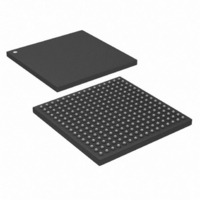
DS33X161+ Maxim Integrated Products, DS33X161+ Datasheet - Page 26

DS33X161+
Manufacturer Part Number
DS33X161+
Description
IC MAPPING ETHERNET 256CSBGA
Manufacturer
Maxim Integrated Products
Datasheet
1.DS33X11.pdf
(375 pages)
Specifications of DS33X161+
Applications
Data Transport
Interface
Parallel/Serial
Voltage - Supply
1.8V, 2.5V, 3.3V
Package / Case
256-CSBGA
Mounting Type
Surface Mount
Lead Free Status / RoHS Status
Lead free / RoHS Compliant
- Current page: 26 of 375
- Download datasheet (3Mb)
Rev: 063008
TCLK1/TMCLK1
________________________________________________ DS33X162/X161/X82/X81/X42/X41/X11/W41/W11
SD_CLKEN
SD_UDQS
SD_LDQS
TDATA10
TDATA11
TDATA12
TDATA13
TDATA14
TDATA15
TDATA16
SD_UDM
SD_LDM
SD_CLK
SD_CLK
TDATA1
TDATA2
TDATA3
TDATA4
TDATA5
TDATA6
TDATA7
TDATA8
TDATA9
TCLK2
TCLK3
TCLK4
NAME
SCAS
SRAS
SWE
PACKAGE PINS
D13
C13
N10
R11
N11
R12
P14
P12
N12
P11
256
M5
D7
D8
C4
N9
N6
N7
R9
R5
R8
A6
B7
A7
A8
A9
T6
T7
P6
P5
P9
144
M3
B5
D5
C5
E7
E6
E8
D7
A8
A7
E5
L3
—
—
—
—
—
—
—
—
—
—
—
—
—
—
—
—
—
—
TYPE
IOz
IOz
O
O
O
O
O
O
O
O
O
I
SERIAL INTERFACE IO PINS
SDRAM Row Address Strobe. Active-low output, used to latch the row
address on rising edge of SD_CLK. It is used with commands for Bank
Activate, Precharge, and Mode Register Write.
SDRAM Column Address Strobe. Active low output, used to latch the
column address on the rising edge of SD_CLK. It is used with commands
for Bank Activate, Precharge, and Mode Register Write.
SDRAM Write Enable. This active low output enables write operation and
auto precharge.
SDRAM Upper Data Mask. SD_UDM is an active high output mask
signal for write data. SD_UDM is updated on both edges of SD_UDQS.
SD_UDM corresponds to data on SDATA15-SDATA8.
SDRAM Lower Data Mask. SD_LDM is an active high output mask signal
for write data. SD_LDM is updated on both edges of SD_LDQS. SD_LDM
corresponds to data on SDATA7-SDATA0.
Lower Data Strobe. Output with write data, input with read data.
SD_LDQS corresponds to data on SDATA7-SDATA0.
Upper Data Strobe. Output with write data, input with read data.
SD_UDQS corresponds to data on SDATA15-SDATA8.
SDRAM Clock. SD_CLK and SD_CLK are differential clock outputs. All
address and control input signals are sampled on the crossing of the
positive edge of SD_CLK and negative edge of SD_CLK. Output (write)
data is referenced to the crossings of SD_CLK and SD_CLK (both
directions of crossing).
SDRAM Clock (Inverted). SD_CLK and SD_CLK are differential clock
outputs. All address and control input signals are sampled on the crossing
of the positive edge of SD_CLK and negative edge of SD_CLK. Output
(write) data is referenced to the crossings of SD_CLK and SD_CLK (both
directions of crossing).
SDRAM Clock Enable. Active High. SD_CLKEN must be active
throughout DDR SDRAM READ and WRITE accesses.
Transmit Serial Data Output. Output on the rising edge of TCLK. The
maximum data rate is 52Mbps.
Not all serial port signals are available on all products in the device family.
Unused output pins should not be connected.
DS33X41/X42/W41/W11: TDATA5 – TDATA16 not used.
DS33X81/X82: TDATA9 – TDATA16 not used.
Serial Interface Transmit Clock Input (TCLK[1:8]).The clock reference
for TDATA, which is output on the rising edge of the clock. TCLK supports
gapped clocking, up to a maximum frequency of 52MHz.
Note that TCLK1 is also TMCLK1, TCLK5 is also TMCLK2. TMCLK3
and TMCLK4 are stand-alone pins.
FUNCTION
26 of 375
Related parts for DS33X161+
Image
Part Number
Description
Manufacturer
Datasheet
Request
R

Part Number:
Description:
MAX7528KCWPMaxim Integrated Products [CMOS Dual 8-Bit Buffered Multiplying DACs]
Manufacturer:
Maxim Integrated Products
Datasheet:

Part Number:
Description:
Single +5V, fully integrated, 1.25Gbps laser diode driver.
Manufacturer:
Maxim Integrated Products
Datasheet:

Part Number:
Description:
Single +5V, fully integrated, 155Mbps laser diode driver.
Manufacturer:
Maxim Integrated Products
Datasheet:

Part Number:
Description:
VRD11/VRD10, K8 Rev F 2/3/4-Phase PWM Controllers with Integrated Dual MOSFET Drivers
Manufacturer:
Maxim Integrated Products
Datasheet:

Part Number:
Description:
Highly Integrated Level 2 SMBus Battery Chargers
Manufacturer:
Maxim Integrated Products
Datasheet:

Part Number:
Description:
Current Monitor and Accumulator with Integrated Sense Resistor; ; Temperature Range: -40°C to +85°C
Manufacturer:
Maxim Integrated Products

Part Number:
Description:
TSSOP 14/A�/RS-485 Transceivers with Integrated 100O/120O Termination Resis
Manufacturer:
Maxim Integrated Products

Part Number:
Description:
TSSOP 14/A�/RS-485 Transceivers with Integrated 100O/120O Termination Resis
Manufacturer:
Maxim Integrated Products

Part Number:
Description:
QFN 16/A�/AC-DC and DC-DC Peak-Current-Mode Converters with Integrated Step
Manufacturer:
Maxim Integrated Products

Part Number:
Description:
TDFN/A/65V, 1A, 600KHZ, SYNCHRONOUS STEP-DOWN REGULATOR WITH INTEGRATED SWI
Manufacturer:
Maxim Integrated Products

Part Number:
Description:
Integrated Temperature Controller f
Manufacturer:
Maxim Integrated Products

Part Number:
Description:
SOT23-6/I�/45MHz to 650MHz, Integrated IF VCOs with Differential Output
Manufacturer:
Maxim Integrated Products

Part Number:
Description:
SOT23-6/I�/45MHz to 650MHz, Integrated IF VCOs with Differential Output
Manufacturer:
Maxim Integrated Products

Part Number:
Description:
EVALUATION KIT/2.4GHZ TO 2.5GHZ 802.11G/B RF TRANSCEIVER WITH INTEGRATED PA
Manufacturer:
Maxim Integrated Products

Part Number:
Description:
QFN/E/DUAL PCIE/SATA HIGH SPEED SWITCH WITH INTEGRATED BIAS RESISTOR
Manufacturer:
Maxim Integrated Products
Datasheet:


