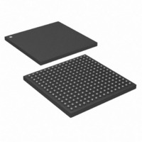
DS33X161+ Maxim Integrated Products, DS33X161+ Datasheet - Page 7

DS33X161+
Manufacturer Part Number
DS33X161+
Description
IC MAPPING ETHERNET 256CSBGA
Manufacturer
Maxim Integrated Products
Datasheet
1.DS33X11.pdf
(375 pages)
Specifications of DS33X161+
Applications
Data Transport
Interface
Parallel/Serial
Voltage - Supply
1.8V, 2.5V, 3.3V
Package / Case
256-CSBGA
Mounting Type
Surface Mount
Lead Free Status / RoHS Status
Lead free / RoHS Compliant
- Current page: 7 of 375
- Download datasheet (3Mb)
________________________________________________ DS33X162/X161/X82/X81/X42/X41/X11/W41/W11
Figure 11-19. GMII Receive Interface Functional Timing ........................................................................................ 336
Figure 11-20. MII Transmit Functional Timing......................................................................................................... 337
Figure 11-21. MII Transmit Half Duplex with a Collision Functional Timing ............................................................ 337
Figure 11-22. MII Receive Functional Timing.......................................................................................................... 337
Figure 11-23. RMII Transmit Interface Functional Timing ....................................................................................... 338
Figure 11-24. RMII Receive Interface Functional Timing ........................................................................................ 338
Figure 12-1. Transmit GMII Interface Timing........................................................................................................... 342
Figure 12-2. Receive GMII Interface Timing............................................................................................................ 343
Figure 12-3. Transmit MII Interface Timing ............................................................................................................. 344
Figure 12-4. Receive MII Interface Timing .............................................................................................................. 345
Figure 12-5. Transmit RMII Interface Timing........................................................................................................... 346
Figure 12-6. Receive RMII Interface Timing............................................................................................................ 347
Figure 12-7. MDIO Interface Timing ........................................................................................................................ 348
Figure 12-8. Transmit WAN Timing (Noninverted TCLK) ........................................................................................ 349
Figure 12-9. Receive WAN Timing (Noninverted RCLK) ........................................................................................ 350
Figure 12-10. Transmit Voice Port Interface Timing................................................................................................ 351
Figure 12-11. Receive Voice Port Interface Timing................................................................................................. 352
Figure 12-12. DDR SDRAM Interface Timing.......................................................................................................... 354
Figure 12-13. Intel Bus Read Timing (MODE = 0) .................................................................................................. 356
Figure 12-14. Intel Bus Write Timing (MODE = 0)................................................................................................... 356
Figure 12-15. Motorola Bus Read Timing (MODE = 1) ........................................................................................... 357
Figure 12-16. Motorola Bus Write Timing (MODE = 1) ........................................................................................... 357
Figure 12-17. Multiplexed Intel Bus Read Timing (MODE = 0) ............................................................................... 359
Figure 12-18. Multiplexed Intel Bus Write Timing (MODE = 0) ............................................................................... 359
Figure 12-19. Multiplexed Motorola Bus Read Timing (MODE = 1)........................................................................ 360
Figure 12-20. Multiplexed Motorola Bus Write Timing (MODE = 1) ........................................................................ 360
Figure 12-21. SPI Interface Timing Diagram ........................................................................................................... 361
Figure 12-22. JTAG Interface Timing ...................................................................................................................... 362
Figure 13-1. JTAG Functional Block Diagram ......................................................................................................... 363
Figure 13-2. TAP Controller State Diagram............................................................................................................. 366
Figure 13-3. JTAG Functional Timing...................................................................................................................... 369
Rev: 063008
7 of 375
Related parts for DS33X161+
Image
Part Number
Description
Manufacturer
Datasheet
Request
R

Part Number:
Description:
MAX7528KCWPMaxim Integrated Products [CMOS Dual 8-Bit Buffered Multiplying DACs]
Manufacturer:
Maxim Integrated Products
Datasheet:

Part Number:
Description:
Single +5V, fully integrated, 1.25Gbps laser diode driver.
Manufacturer:
Maxim Integrated Products
Datasheet:

Part Number:
Description:
Single +5V, fully integrated, 155Mbps laser diode driver.
Manufacturer:
Maxim Integrated Products
Datasheet:

Part Number:
Description:
VRD11/VRD10, K8 Rev F 2/3/4-Phase PWM Controllers with Integrated Dual MOSFET Drivers
Manufacturer:
Maxim Integrated Products
Datasheet:

Part Number:
Description:
Highly Integrated Level 2 SMBus Battery Chargers
Manufacturer:
Maxim Integrated Products
Datasheet:

Part Number:
Description:
Current Monitor and Accumulator with Integrated Sense Resistor; ; Temperature Range: -40°C to +85°C
Manufacturer:
Maxim Integrated Products

Part Number:
Description:
TSSOP 14/A�/RS-485 Transceivers with Integrated 100O/120O Termination Resis
Manufacturer:
Maxim Integrated Products

Part Number:
Description:
TSSOP 14/A�/RS-485 Transceivers with Integrated 100O/120O Termination Resis
Manufacturer:
Maxim Integrated Products

Part Number:
Description:
QFN 16/A�/AC-DC and DC-DC Peak-Current-Mode Converters with Integrated Step
Manufacturer:
Maxim Integrated Products

Part Number:
Description:
TDFN/A/65V, 1A, 600KHZ, SYNCHRONOUS STEP-DOWN REGULATOR WITH INTEGRATED SWI
Manufacturer:
Maxim Integrated Products

Part Number:
Description:
Integrated Temperature Controller f
Manufacturer:
Maxim Integrated Products

Part Number:
Description:
SOT23-6/I�/45MHz to 650MHz, Integrated IF VCOs with Differential Output
Manufacturer:
Maxim Integrated Products

Part Number:
Description:
SOT23-6/I�/45MHz to 650MHz, Integrated IF VCOs with Differential Output
Manufacturer:
Maxim Integrated Products

Part Number:
Description:
EVALUATION KIT/2.4GHZ TO 2.5GHZ 802.11G/B RF TRANSCEIVER WITH INTEGRATED PA
Manufacturer:
Maxim Integrated Products

Part Number:
Description:
QFN/E/DUAL PCIE/SATA HIGH SPEED SWITCH WITH INTEGRATED BIAS RESISTOR
Manufacturer:
Maxim Integrated Products
Datasheet:


