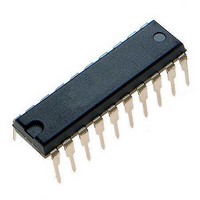
L9705 STMicroelectronics, L9705 Datasheet - Page 5

L9705
Manufacturer Part Number
L9705
Description
IC INTERFACE DOUBLE QUAD 20-DIP
Manufacturer
STMicroelectronics
Datasheet
1.L9705.pdf
(8 pages)
Specifications of L9705
Applications
Monitoring, Digital Current
Voltage - Supply
5 V ~ 25 V
Package / Case
20-DIP (0.300", 7.62mm)
Mounting Type
Through Hole
Mounting Style
Through Hole
Lead Free Status / RoHS Status
Lead free / RoHS Compliant
Interface
-
Lead Free Status / Rohs Status
Lead free / RoHS Compliant
Available stocks
Company
Part Number
Manufacturer
Quantity
Price
Part Number:
L9705D
Manufacturer:
ST
Quantity:
20 000
Company:
Part Number:
L9705D013TR
Manufacturer:
OSRAM
Quantity:
5 149
The L9705 circuit compares the input current with the current through the internal reference resistor. The
device is designed to work with an external input series resistor of R
the contact current, when the contact is closed and the device activated (EN =LOW) is:
For this calculation the limit value of the V
the lowest limit value of I
Figure 4. The output voltage as a function of the input resistance at the corresponding sense input.
The function of the circuit can be demonstrated with the transfer characteristics, showing the output status
as a function of the input resistor R
tact resistance R
R
and for the open contact:
R
The output goes HIGH when the input resistance increases above 5.3K
(V
4.8K (V
= 1.8K
29K (V
as ON = LOW and a contact with R
as OFF = HIGH.
These limits are valid within the supply voltage range 6V
verse battery protection diode D1 voltage from 0.5V to 1V.
The internal clamping diodes at the contact monitoring inputs together with the external contacts series
resistors R
limits the input current at the transient.
The dynamic behaviour of the circuit is defined with the times t
input capacitor C
influenced also with the time constant R
The delay time t
output external capacitance less than 50pF is assumed, the internal output capacitance of the tristate buff-
ers are less than 5pF.
V
I
I
BAT
= R
= R
GND
IN
IN
contacts) and goes LOW, when the input resistance decreases below 4K
= 0.1V
BAT
+ R
+ R
BAT
(GND contacts) and R
IN
CON
COFF
contacts) for HIGH implies that a contact with R
contacts); these values are typical values for the switching thresholds. The limit values of R
allows to withstand the transients at the contact connection.The contact series resistor R
S
, the battery voltage potential difference of V
, (3)
dTS
CON
, (4)
IN
must be charged through the resistor R
, when disabling the device, is defined only with the internal circuitry. In both cases,
or R
IN
COFF
is calculated in (1) and (2)
I
IN
, for the closed contact:
=
I
= 1.8K
I
V
----------------------------------------------------
COFF
IN
I
, shown in figure 4. The input resistor is a sum of the R
BAT
=
= 19K (GND contacts) or 28K (V
IN
V
-------------------- -
+
S
C
S
1k
1 k
(V
to V
IN
V
–
BAT
BAT
.
2V
IN
contacts) for LOW and R
and V
, for GND contacts, (1)
–
2 V
IN
, fro V
saturation voltage of 2V was considered so that
IN
CON
V
. In this case the total delay time tdo may be
BAT
BAT
S
do
= 100 ( at I
contacts, (2)
and t
16V, the ground potential difference of
< 0.1V
IN1-8
dTS
BAT
. When the contact is open, the
(GND contacts) or 6.5K
= 1K . With this input resistor
I
BAT
IN
= 20K
= 10mA) will be recognized
and the variation of the re-
contact) will be recognized
(GND contacts) and
(GND contacts) or
IN
and the con-
L9705
5/8
IN
I


