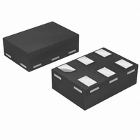
74LVC1G66GM,115 NXP Semiconductors, 74LVC1G66GM,115 Datasheet - Page 15

74LVC1G66GM,115
Manufacturer Part Number
74LVC1G66GM,115
Description
IC SWITCH SPST 6XSON
Manufacturer
NXP Semiconductors
Series
74LVCr
Type
Analog Switchr
Datasheet
1.74LVC1G66GM115.pdf
(25 pages)
Specifications of 74LVC1G66GM,115
Package / Case
6-XFDFN
Function
Switch
Circuit
1 x SPST- NO
On-state Resistance
6 Ohm
Voltage Supply Source
Single Supply
Voltage - Supply, Single/dual (±)
1.65 V ~ 5.5 V
Current - Supply
0.1µA
Operating Temperature
-40°C ~ 125°C
Mounting Type
Surface Mount
Number Of Switches
1
Switch Configuration
SPST
On Resistance (max)
34 Ohm (Typ) @ 1.95 V
On Time (max)
5.3 ns (Typ) @ 1.95 V
Off Time (max)
4.2 ns (Typ) @ 1.95 V
Off Isolation (typ)
- 46 dB
Supply Voltage (max)
5.5 V
Supply Voltage (min)
1.65 V
Supply Current
100 mA
Maximum Power Dissipation
250 mW
Maximum Operating Temperature
+ 125 C
Mounting Style
SMD/SMT
Minimum Operating Temperature
- 40 C
Off State Leakage Current (max)
200 uA
Propagation Delay Time
1 ns
Switch Current (typ)
0.0001 mA @ 3.3 V
Package
6XSON
Maximum On Resistance
195@1.95V Ohm
Maximum Propagation Delay Bus To Bus
0.8(Typ)@1.95V|0.4(Typ)@2.7V|0.3(Typ)@3.6V|0.2(Typ)@5.5V ns
Maximum Low Level Output Current
50 mA
Maximum Turn-off Time
4.2(Typ)@1.95V ns
Maximum Turn-on Time
5.3(Typ)@1.95V ns
Switch Architecture
SPST
Power Supply Type
Single
Lead Free Status / RoHS Status
Lead free / RoHS Compliant
Lead Free Status / RoHS Status
Lead free / RoHS Compliant, Lead free / RoHS Compliant
Other names
568-4406-2
74LVC1G66GM-G
74LVC1G66GM-G
935284306115
74LVC1G66GM-G
74LVC1G66GM-G
935284306115
NXP Semiconductors
74LVC1G66
Product data sheet
Fig 21. Test circuit for measuring isolation (OFF-state)
Fig 22. Test circuit for measuring crosstalk between digital input and switch
Fig 23. Test circuit for measuring charge injection
Adjust f
Q
ΔV
R
V
gen
gen
inj
O
= ΔV
= output voltage variation.
= generator voltage.
= generator resistance.
i
voltage to obtain 0 dBm level at input.
O
× C
L
.
G
G
input (E)
f i
logic
V
logic
input
logic
input
O
0.1 μF
50 Ω
All information provided in this document is subject to legal disclaimers.
0.5V
50 Ω
R gen
off
V gen
0.5V
CC
R L
CC
V
Rev. 7 — 30 July 2010
600 Ω
IL
Y/Z
Y/Z
Y/Z
E
E
E
V
V
CC
CC
V
CC
on
Z/Y
Z/Y
Z/Y
0.5V
CC
R L
1 MΩ
R L
C L
0.5V
001aam398
dB
C L
C L
0.1 nF
001aam395
001aam396
CC
R L
off
001aam394
ΔV
O
V
V
O
O
V
O
74LVC1G66
© NXP B.V. 2010. All rights reserved.
Bilateral switch
15 of 25


