NX3V1G66GM,115 NXP Semiconductors, NX3V1G66GM,115 Datasheet - Page 12
NX3V1G66GM,115
Manufacturer Part Number
NX3V1G66GM,115
Description
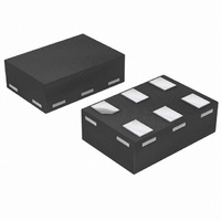
IC SWITCH SPST 6XSON
Manufacturer
NXP Semiconductors
Datasheet
1.NX3V1G66GM115.pdf
(18 pages)
Specifications of NX3V1G66GM,115
Package / Case
6-XFDFN
Function
Switch
Circuit
1 x SPST- NO
On-state Resistance
250 mOhm
Voltage Supply Source
Single Supply
Voltage - Supply, Single/dual (±)
1.4 V ~ 4.3 V
Current - Supply
150nA
Operating Temperature
-40°C ~ 125°C
Mounting Type
Surface Mount
Switch Configuration
SPST
On Resistance (max)
0.8 Ohm (Typ) @ 1.4 V
On Time (max)
42 ns @ 1.6 V
Off Time (max)
22 ns @ 1.6 V
Supply Voltage (max)
3.6 V
Supply Voltage (min)
1.4 V
Maximum Power Dissipation
250 mW
Maximum Operating Temperature
+ 125 C
Mounting Style
SMD/SMT
Minimum Operating Temperature
- 40 C
Switch Current (typ)
0.00069 mA @ 3.6 V
Lead Free Status / RoHS Status
Lead free / RoHS Compliant
Lead Free Status / RoHS Status
Lead free / RoHS Compliant, Lead free / RoHS Compliant
Other names
568-4645-2
935285903115
NX3V1G66GM-G
935285903115
NX3V1G66GM-G


NXP Semiconductors
NX3V1G66
Product data sheet
Fig 20. Test circuit for measuring crosstalk voltage between digital input and switch
Fig 21. Test circuit for measuring charge injection
b. Input and output pulse definitions
a. Test circuit.
b. Input and output pulse definitions.
Definition: Q
V
R
V
gen
gen
O
= output voltage variation.
= generator voltage.
= generator resistance.
inj
= V
O
C
L
G
.
V I
input (E)
input (E)
logic
V
logic
V
All information provided in this document is subject to legal disclaimers.
O
V
V O
O
off
off
R L
Rev. 6 — 21 December 2010
Y/Z
C L
E
on
V
on
CC
Low-ohmic single-pole single-throw analog switch
GND
Z/Y
off
R
gen
001aah384
001aah381
off
V
O
V
001aah385
ct
V
gen
NX3V1G66
© NXP B.V. 2010. All rights reserved.
12 of 18
Related parts for NX3V1G66GM,115
Image
Part Number
Description
Manufacturer
Datasheet
Request
R

Part Number:
Description:
Low-voltage Analog Switch
Manufacturer:
NXP Semiconductors
Datasheet:
Part Number:
Description:
NXP Semiconductors designed the LPC2420/2460 microcontroller around a 16-bit/32-bitARM7TDMI-S CPU core with real-time debug interfaces that include both JTAG andembedded trace
Manufacturer:
NXP Semiconductors
Datasheet:

Part Number:
Description:
NXP Semiconductors designed the LPC2458 microcontroller around a 16-bit/32-bitARM7TDMI-S CPU core with real-time debug interfaces that include both JTAG andembedded trace
Manufacturer:
NXP Semiconductors
Datasheet:
Part Number:
Description:
NXP Semiconductors designed the LPC2468 microcontroller around a 16-bit/32-bitARM7TDMI-S CPU core with real-time debug interfaces that include both JTAG andembedded trace
Manufacturer:
NXP Semiconductors
Datasheet:
Part Number:
Description:
NXP Semiconductors designed the LPC2470 microcontroller, powered by theARM7TDMI-S core, to be a highly integrated microcontroller for a wide range ofapplications that require advanced communications and high quality graphic displays
Manufacturer:
NXP Semiconductors
Datasheet:
Part Number:
Description:
NXP Semiconductors designed the LPC2478 microcontroller, powered by theARM7TDMI-S core, to be a highly integrated microcontroller for a wide range ofapplications that require advanced communications and high quality graphic displays
Manufacturer:
NXP Semiconductors
Datasheet:
Part Number:
Description:
The Philips Semiconductors XA (eXtended Architecture) family of 16-bit single-chip microcontrollers is powerful enough to easily handle the requirements of high performance embedded applications, yet inexpensive enough to compete in the market for hi
Manufacturer:
NXP Semiconductors
Datasheet:
Part Number:
Description:
The XA-S3 device is a member of Philips Semiconductors? XA(eXtended Architecture) family of high performance 16-bitsingle-chip microcontrollers
Manufacturer:
NXP Semiconductors
Datasheet:

Part Number:
Description:
The NXP BlueStreak LH75401/LH75411 family consists of two low-cost 16/32-bit System-on-Chip (SoC) devices
Manufacturer:
NXP Semiconductors
Datasheet:
Part Number:
Description:
The NXP LPC3130/3131 combine an 180 MHz ARM926EJ-S CPU core, high-speed USB2
Manufacturer:
NXP Semiconductors
Datasheet:
Part Number:
Description:
The NXP LPC3141 combine a 270 MHz ARM926EJ-S CPU core, High-speed USB 2
Manufacturer:
NXP Semiconductors
Part Number:
Description:
The NXP LPC3143 combine a 270 MHz ARM926EJ-S CPU core, High-speed USB 2
Manufacturer:
NXP Semiconductors

Part Number:
Description:
The NXP LPC3152 combines an 180 MHz ARM926EJ-S CPU core, High-speed USB 2
Manufacturer:
NXP Semiconductors
Part Number:
Description:
The NXP LPC3154 combines an 180 MHz ARM926EJ-S CPU core, High-speed USB 2
Manufacturer:
NXP Semiconductors