ADG409BNZ Analog Devices Inc, ADG409BNZ Datasheet - Page 4
ADG409BNZ
Manufacturer Part Number
ADG409BNZ
Description
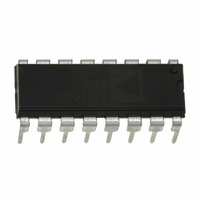
IC MULTIPLEXER DUAL 4X1 16DIP
Manufacturer
Analog Devices Inc
Series
LC²MOSr
Type
Analog Multiplexerr
Datasheet
1.ADG408BNZ.pdf
(16 pages)
Specifications of ADG409BNZ
Function
Multiplexer
Circuit
2 x 4:1
On-state Resistance
100 Ohm
Voltage Supply Source
Single Supply
Voltage - Supply, Single/dual (±)
5V, 12V
Current - Supply
100µA
Operating Temperature
-40°C ~ 85°C
Mounting Type
Through Hole
Package / Case
16-DIP (0.300", 7.62mm)
No. Of Circuits
2
Supply Current
100µA
On State Resistance Max
40ohm
Supply Voltage Range
12V, ± 15V
Operating Temperature Range
-40°C To +85°C
Analog Switch Case Style
DIP
Package
16PDIP
Maximum On Resistance
100@±15V Ohm
Maximum Propagation Delay Bus To Bus
130(Typ)@12V@-40C to 85C|250@±15V@-40C to 85C ns
Maximum High Level Output Current
20 mA
Multiplexer Architecture
4:1
Maximum Turn-off Time
60(Typ)@12V ns
Maximum Turn-on Time
150@±15V ns
Power Supply Type
Single|Dual
Multiplexer Configuration
Dual 4:1
Number Of Inputs
8
Number Of Outputs
2
Number Of Channels
2
Analog Switch On Resistance
100@±15VOhm
Analog Switch Turn On Time
150ns
Analog Switch Turn Off Time
60ns
Package Type
PDIP
Power Supply Requirement
Single/Dual
Single Supply Voltage (min)
5V
Single Supply Voltage (typ)
12V
Single Supply Voltage (max)
12V
Dual Supply Voltage (typ)
±15V
Dual Supply Voltage (max)
±22V
Power Dissipation
470mW
Mounting
Through Hole
Pin Count
16
Operating Temp Range
-40C to 85C
Operating Temperature Classification
Industrial
Lead Free Status / RoHS Status
Lead free / RoHS Compliant
Lead Free Status / RoHS Status
Lead free / RoHS Compliant, Lead free / RoHS Compliant
Available stocks
Company
Part Number
Manufacturer
Quantity
Price
Company:

Part Number:
ADG409BNZ
Manufacturer:
NXP
Quantity:
677
Part Number:
ADG409BNZ
Manufacturer:
ADI/亚德诺
Quantity:
20 000


ADG408/ADG409
Parameter
POWER REQUIREMENTS
1
SINGLE SUPPLY
V
Table 2.
Parameter
ANALOG SWITCH
LEAKAGE CURRENTS
DIGITAL INPUTS
DYNAMIC CHARACTERISTICS
Guaranteed by design, not subject to production test.
DD
I
I
I
Analog Signal Range
R
Source Off Leakage I
Drain Off Leakage I
Channel On Leakage I
Input High Voltage, V
Input Low Voltage, V
Input Current
C
t
t
t
t
Charge Injection
Off Isolation
DD
SS
DD
TRANSITION
OPEN
ON
OFF
ON
IN,
= 12 V, V
ADG408
ADG409
ADG408
ADG409
I
INL
(EN)
Digital Input Capacitance
(EN)
or I
INH
SS
= 0 V, GND = 0 V, unless otherwise noted.
D
S
INL
(OFF)
INH
(OFF)
D
, I
S
(ON)
1
+25ºC
100
200
+25ºC
90
±0.5
±1
±1
±1
±1
8
130
10
140
60
5
–75
B Version
B Version
−40ºC to
+85ºC
0 to V
±50
±100
±50
±100
±50
2.4
0.8
±10
−40ºC to
+85ºC
1
5
1
5
500
DD
+25°C
90
±0.5
±1
±1
±1
±1
130
10
140
60
5
–75
8
+25ºC
100
200
Rev. C | Page 4 of 16
T Version
T Version
−55ºC to
+125ºC
1
5
1
5
500
−55ºC to
+125ºC
0 to V
±50
±100
±50
±100
±50
2.4
0.8
±10
DD
Unit
μA typ
μA max
μA typ
μA max
μA typ
μA max
V
Ω typ
nA max
nA max
nA max
nA max
nA max
V min
V max
μA max
ns typ
ns typ
ns typ
ns typ
pC typ
dB typ
Unit
pF typ
Test Conditions/Comments
V
V
Test Conditions/Comments
V
V
V
V
f = 1 MHz
R
V
R
V
R
V
R
V
V
R
V
VD = 8 V/0 V, V
IN
IN
D
D
S
IN
L
S1
L
S
L
S
L
S
S
L
EN
= 1 kΩ f = 100 kHz;
= 300 Ω, C
= 300 Ω, C
= 300 Ω C
= 300 Ω, C
= 3 V, 10 V, I
= V
= 5 V; see Figure 23
= 5 V; see Figure 24
= 5 V; see Figure 24
= 0 V, R
= 8 V/0 V, V
= 0 V, V
= 0 V, V
= 0 or V
= 8 V/0 V, V
= 0 V; see Figure 26
D
= 8 V/0 V; see Figure 21
S
EN
EN
DD
= 0Ω, C
= 0 V
= 2.4 V
L
L
L
L
= 35 pF;
S
= 35 pF;
= 35 pF;
= 35 pF;
S
S8
S
= 0 V/8 V; see Figure 20
= –1 mA
= 0 V/8 V; see Figure 19
= 0 V/8 V; see Figure 22
L
= 10 nF; see Figure 25
Related parts for ADG409BNZ
Image
Part Number
Description
Manufacturer
Datasheet
Request
R

Part Number:
Description:
±1.7g Dual-Axis IMEMS Accelerometer Evaluation Board
Manufacturer:
Analog Devices Inc
Datasheet:

Part Number:
Description:
Inertial Sensor Evaluation System
Manufacturer:
Analog Devices Inc
Datasheet:
Part Number:
Description:
Manufacturer:
Analog Devices Inc
Datasheet:
Part Number:
Description:
Manufacturer:
Analog Devices Inc
Datasheet:
Part Number:
Description:
Manufacturer:
Analog Devices Inc
Datasheet:
Part Number:
Description:
Manufacturer:
Analog Devices Inc
Datasheet:
Part Number:
Description:
Manufacturer:
Analog Devices Inc
Datasheet:
Part Number:
Description:
Manufacturer:
Analog Devices Inc
Datasheet:
Part Number:
Description:
Manufacturer:
Analog Devices Inc
Datasheet:
Part Number:
Description:
Manufacturer:
Analog Devices Inc
Datasheet:
Part Number:
Description:
Manufacturer:
Analog Devices Inc
Datasheet:
Part Number:
Description:
Manufacturer:
Analog Devices Inc
Datasheet:
Part Number:
Description:
Manufacturer:
Analog Devices Inc
Datasheet: