ADG409BNZ Analog Devices Inc, ADG409BNZ Datasheet - Page 6
ADG409BNZ
Manufacturer Part Number
ADG409BNZ
Description
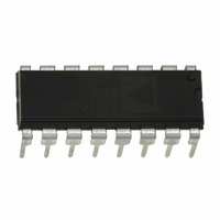
IC MULTIPLEXER DUAL 4X1 16DIP
Manufacturer
Analog Devices Inc
Series
LC²MOSr
Type
Analog Multiplexerr
Datasheet
1.ADG408BNZ.pdf
(16 pages)
Specifications of ADG409BNZ
Function
Multiplexer
Circuit
2 x 4:1
On-state Resistance
100 Ohm
Voltage Supply Source
Single Supply
Voltage - Supply, Single/dual (±)
5V, 12V
Current - Supply
100µA
Operating Temperature
-40°C ~ 85°C
Mounting Type
Through Hole
Package / Case
16-DIP (0.300", 7.62mm)
No. Of Circuits
2
Supply Current
100µA
On State Resistance Max
40ohm
Supply Voltage Range
12V, ± 15V
Operating Temperature Range
-40°C To +85°C
Analog Switch Case Style
DIP
Package
16PDIP
Maximum On Resistance
100@±15V Ohm
Maximum Propagation Delay Bus To Bus
130(Typ)@12V@-40C to 85C|250@±15V@-40C to 85C ns
Maximum High Level Output Current
20 mA
Multiplexer Architecture
4:1
Maximum Turn-off Time
60(Typ)@12V ns
Maximum Turn-on Time
150@±15V ns
Power Supply Type
Single|Dual
Multiplexer Configuration
Dual 4:1
Number Of Inputs
8
Number Of Outputs
2
Number Of Channels
2
Analog Switch On Resistance
100@±15VOhm
Analog Switch Turn On Time
150ns
Analog Switch Turn Off Time
60ns
Package Type
PDIP
Power Supply Requirement
Single/Dual
Single Supply Voltage (min)
5V
Single Supply Voltage (typ)
12V
Single Supply Voltage (max)
12V
Dual Supply Voltage (typ)
±15V
Dual Supply Voltage (max)
±22V
Power Dissipation
470mW
Mounting
Through Hole
Pin Count
16
Operating Temp Range
-40C to 85C
Operating Temperature Classification
Industrial
Lead Free Status / RoHS Status
Lead free / RoHS Compliant
Lead Free Status / RoHS Status
Lead free / RoHS Compliant, Lead free / RoHS Compliant
Available stocks
Company
Part Number
Manufacturer
Quantity
Price
Company:

Part Number:
ADG409BNZ
Manufacturer:
NXP
Quantity:
677
Part Number:
ADG409BNZ
Manufacturer:
ADI/亚德诺
Quantity:
20 000


ADG408/ADG409
ABSOLUTE MAXIMUM RATINGS
T
Table 3.
Parameter
V
V
V
Analog, Digital Inputs
Continuous Current, S or D
Peak Current, S or D
Operating Temperature Range
Junction Temperature
CERDIP Package, Power Dissipation
PDIP Package, Power Dissipation
TSSOP Package, Power Dissipation
SOIC Package, Power Dissipation
DD
DD
SS
A
(Pulsed at 1 ms, 10% Duty Cycle
Maximum)
Industrial (B Version)
Extended (T Version)
Storage Temperature Range
θ
Lead Temperature, Soldering
(10 sec)
θ
Lead Temperature, Soldering
(10 sec)
θ
θ
θ
Lead Temperature, Soldering
= 25°C, unless otherwise noted.
to GND
to V
to GND
JA
JA,
JA
JC
JA
, Thermal Impedance
, Thermal Impedance
, Thermal Impedance
, Thermal Impedance
Thermal Impedance
Vapor Phase (60 sec)
Infrared (15 sec)
SS
Rating
44 V
−0.3 V to +32 V
+0.3 V to −32 V
V
20 mA
40 mA
−40° C to +85°C
−55° C to +125°C
−65° C to +150°C
150°C
900 mW
76°C/W
300°C
470 mW
117°C/W
260°C
450 mW
155°C/W
50°C/W
600 mW
77°C/W
215°C
220°C
SS
whichever occurs first
− 2 V to V
DD
+ 2 V or 20 mA,
Rev. C | Page 6 of 16
Stresses above those listed under Absolute Maximum Ratings
may cause permanent damage to the device. This is a stress
rating only; functional operation of the device at these or any
other conditions above those indicated in the operational
section of this specification is not implied. Exposure to absolute
maximum rating conditions for extended periods may affect
device reliability.
ESD CAUTION
Related parts for ADG409BNZ
Image
Part Number
Description
Manufacturer
Datasheet
Request
R

Part Number:
Description:
±1.7g Dual-Axis IMEMS Accelerometer Evaluation Board
Manufacturer:
Analog Devices Inc
Datasheet:

Part Number:
Description:
Inertial Sensor Evaluation System
Manufacturer:
Analog Devices Inc
Datasheet:
Part Number:
Description:
Manufacturer:
Analog Devices Inc
Datasheet:
Part Number:
Description:
Manufacturer:
Analog Devices Inc
Datasheet:
Part Number:
Description:
Manufacturer:
Analog Devices Inc
Datasheet:
Part Number:
Description:
Manufacturer:
Analog Devices Inc
Datasheet:
Part Number:
Description:
Manufacturer:
Analog Devices Inc
Datasheet:
Part Number:
Description:
Manufacturer:
Analog Devices Inc
Datasheet:
Part Number:
Description:
Manufacturer:
Analog Devices Inc
Datasheet:
Part Number:
Description:
Manufacturer:
Analog Devices Inc
Datasheet:
Part Number:
Description:
Manufacturer:
Analog Devices Inc
Datasheet:
Part Number:
Description:
Manufacturer:
Analog Devices Inc
Datasheet:
Part Number:
Description:
Manufacturer:
Analog Devices Inc
Datasheet: