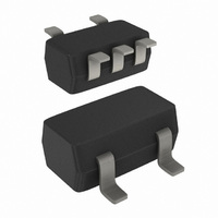
74LVC1G384GW,125 NXP Semiconductors, 74LVC1G384GW,125 Datasheet - Page 3

74LVC1G384GW,125
Manufacturer Part Number
74LVC1G384GW,125
Description
IC SWITCH SPST UMT5
Manufacturer
NXP Semiconductors
Series
74LVCr
Type
Analog Switchr
Datasheet
1.74LVC1G384GV125.pdf
(25 pages)
Specifications of 74LVC1G384GW,125
Package / Case
6-TSSOP (5 lead), SC-88A, SOT-353
Function
Switch
Circuit
1 x SPST- NO
On-state Resistance
6 Ohm
Voltage Supply Source
Single Supply
Voltage - Supply, Single/dual (±)
1.65 V ~ 5.5 V
Current - Supply
0.1µA
Operating Temperature
-40°C ~ 125°C
Mounting Type
Surface Mount
Switch Configuration
SPST
On Resistance (max)
34 Ohm (Typ) @ 1.95 V
On Time (max)
10 ns (Typ) @ 1.95 V
Off Time (max)
7.4 ns (Typ) @ 1.95 V
Supply Voltage (max)
5.5 V
Supply Voltage (min)
1.65 V
Maximum Power Dissipation
250 mW
Maximum Operating Temperature
+ 125 C
Mounting Style
SMD/SMT
Minimum Operating Temperature
- 40 C
Switch Current (typ)
0.0001 mA @ 3.3 V
Multiplexer Configuration
Single SPST
Number Of Inputs
1
Number Of Outputs
1
Number Of Channels
1
Analog Switch On Resistance
34@1.95VOhm
Power Supply Requirement
Single
Single Supply Voltage (min)
1.65V
Single Supply Voltage (typ)
3/5V
Single Supply Voltage (max)
5.5V
Dual Supply Voltage (min)
Not RequiredV
Dual Supply Voltage (typ)
Not RequiredV
Dual Supply Voltage (max)
Not RequiredV
Power Dissipation
250mW
Mounting
Surface Mount
Pin Count
5
Operating Temp Range
-40C to 125C
Operating Temperature Classification
Automotive
Lead Free Status / RoHS Status
Lead free / RoHS Compliant
Lead Free Status / RoHS Status
Lead free / RoHS Compliant, Lead free / RoHS Compliant
Other names
74LVC1G384GW-G
74LVC1G384GW-G
935274581125
74LVC1G384GW-G
935274581125
NXP Semiconductors
6. Pinning information
Table 3.
74LVC1G384
Product data sheet
Symbol
Y
Z
GND
E
n.c.
V
Fig 4.
CC
GND
Pin configuration
SOT353-1 and SOT753
Y
Z
Pin description
1
2
3
74LVC1G384
6.1 Pinning
6.2 Pin description
001aaa365
Pin
SOT353-1, SOT753 SOT886, SOT891, SOT1115 and SOT1202
1
2
3
4
-
5
4
5
V CC
E
1
2
3
4
5
6
All information provided in this document is subject to legal disclaimers.
Fig 5.
Rev. 3 — 3 November 2010
GND
Pin configuration SOT886
Y
Z
Transparent top view
74LVC1G384
1
2
3
001aag477
6
5
4
V
n.c.
E
CC
Fig 6.
ground (0 V)
not connected
Description
independent input or output
independent output or input
enable input (active LOW)
supply voltage
GND
Pin configuration SOT891,
SOT1115 and SOT1202
74LVC1G384
Y
Z
Transparent top view
74LVC1G384
1
2
3
© NXP B.V. 2010. All rights reserved.
Bilateral switch
001aag478
6
5
4
V
n.c.
E
CC
3 of 25


