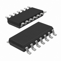
74LVC4066D,118 NXP Semiconductors, 74LVC4066D,118 Datasheet - Page 3

74LVC4066D,118
Manufacturer Part Number
74LVC4066D,118
Description
IC SWITCH QUAD SPST 14SOIC
Manufacturer
NXP Semiconductors
Series
74LVCr
Type
Analog Switchr
Datasheet
1.74LVC4066BQ115.pdf
(23 pages)
Specifications of 74LVC4066D,118
Package / Case
14-SOIC (0.154", 3.90mm Width)
Function
Switch
Circuit
4 x SPST - NO
On-state Resistance
6 Ohm
Voltage Supply Source
Single Supply
Voltage - Supply, Single/dual (±)
1.65 V ~ 5.5 V
Current - Supply
0.1µA
Operating Temperature
-40°C ~ 125°C
Mounting Type
Surface Mount
Switch Configuration
SPST
On Resistance (max)
34 Ohm (Typ) @ 1.95 V
On Time (max)
5.3 ns (Typ) @ 1.95 V
Off Time (max)
4.2 ns (Typ) @ 1.95 V
Supply Voltage (max)
5.5 V
Supply Voltage (min)
1.65 V
Maximum Power Dissipation
500 mW
Maximum Operating Temperature
+ 125 C
Mounting Style
SMD/SMT
Minimum Operating Temperature
- 40 C
Package
14SO
Maximum On Resistance
195@1.95V Ohm
Maximum Propagation Delay Bus To Bus
0.2(Typ)@5.5V|0.3(Typ)@3.6V|0.4(Typ)@2.7V|0.8(Typ)@1.95V ns
Maximum Low Level Output Current
50 mA
Maximum Turn-off Time
4.2(Typ)@1.95V ns
Maximum Turn-on Time
5.3(Typ)@1.95V ns
Switch Architecture
SPST
Power Supply Type
Single
Lead Free Status / RoHS Status
Lead free / RoHS Compliant
Lead Free Status / RoHS Status
Lead free / RoHS Compliant, Lead free / RoHS Compliant
Other names
74LVC4066D-T
74LVC4066D-T
935273717118
74LVC4066D-T
935273717118
NXP Semiconductors
5. Pinning information
Table 2.
74LVC4066
Product data sheet
Symbol
1Y
1Z
2Z
2Y
2E
3E
GND
3Y
3Z
4Z
4Y
4E
1E
V
Fig 4.
CC
Pin configuration for SO14 and TSSOP14
Pin description
GND
1Y
1Z
2Z
2Y
2E
3E
5.1 Pinning
5.2 Pin description
1
2
3
4
5
6
7
Pin
1
2
3
4
5
6
7
8
9
10
11
12
13
14
4066
001aad117
14
13
12
11
10
Description
independent input/output
independent output/input
independent output/input
independent input/output
enable input (active HIGH)
enable input (active HIGH)
ground (0 V)
independent input/output
independent output/input
independent output/input
independent input/output
enable input (active HIGH)
enable input (active HIGH)
supply voltage
9
8
All information provided in this document is subject to legal disclaimers.
V
1E
4E
4Y
4Z
3Z
3Y
CC
Rev. 4 — 24 November 2010
Fig 5.
(1) This is not a supply pin. The substrate is attached to this
pad using conductive die attach material. There is no
electrical or mechanical requirement to solder this pad.
However, if it is soldered, the solder land should remain
floating or be connected to GND.
Pin configuration for DHVQFN14
index area
terminal 1
2Y
2E
3E
1Z
2Z
Transparent top view
2
3
4
5
6
GND
4066
(1)
74LVC4066
Quad bilateral switch
13
12
11
10
9
001aad118
© NXP B.V. 2010. All rights reserved.
1E
4E
4Y
4Z
3Z
3 of 23


