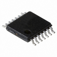
74LVC4066PW,118 NXP Semiconductors, 74LVC4066PW,118 Datasheet - Page 11

74LVC4066PW,118
Manufacturer Part Number
74LVC4066PW,118
Description
IC SWITCH QUAD SPST 14TSSOP
Manufacturer
NXP Semiconductors
Series
74LVCr
Type
Analog Switchr
Datasheet
1.74LVC4066BQ115.pdf
(23 pages)
Specifications of 74LVC4066PW,118
Package / Case
14-TSSOP (0.173", 4.40mm Width)
Function
Switch
Circuit
4 x SPST - NO
On-state Resistance
6 Ohm
Voltage Supply Source
Single Supply
Voltage - Supply, Single/dual (±)
1.65 V ~ 5.5 V
Current - Supply
0.1µA
Operating Temperature
-40°C ~ 125°C
Mounting Type
Surface Mount
Switch Configuration
SPST
On Resistance (max)
34 Ohm (Typ) @ 1.95 V
On Time (max)
5.3 ns (Typ) @ 1.95 V
Off Time (max)
4.2 ns (Typ) @ 1.95 V
Supply Voltage (max)
5.5 V
Supply Voltage (min)
1.65 V
Maximum Power Dissipation
500 mW
Maximum Operating Temperature
+ 125 C
Mounting Style
SMD/SMT
Minimum Operating Temperature
- 40 C
Package
14TSSOP
Maximum On Resistance
195@1.95V Ohm
Maximum Propagation Delay Bus To Bus
0.2(Typ)@5.5V|0.3(Typ)@3.6V|0.4(Typ)@2.7V|0.8(Typ)@1.95V ns
Maximum Low Level Output Current
50 mA
Maximum Turn-off Time
4.2(Typ)@1.95V ns
Maximum Turn-on Time
5.3(Typ)@1.95V ns
Switch Architecture
SPST
Power Supply Type
Single
Lead Free Status / RoHS Status
Lead free / RoHS Compliant
Lead Free Status / RoHS Status
Lead free / RoHS Compliant, Lead free / RoHS Compliant
Other names
74LVC4066PW-T
74LVC4066PW-T
935273718118
74LVC4066PW-T
935273718118
NXP Semiconductors
Table 9.
74LVC4066
Product data sheet
Supply voltage
V
1.65 V to 1.95 V
2.3 V to 2.7 V
2.7 V
3.0 V to 3.6 V
4.5 V to 5.5 V
Fig 15. Input (nY or nZ) to output (nZ or nY) propagation delays
Fig 16. Enable and disable times
CC
Measurement points are given in
Measurement points are given in
Logic levels: V
Logic levels: V
Measurement points
10.1 Waveforms and test circuit
OL
OL
nY or nZ
nY or nZ
and V
and V
Input
V
0.5V
0.5V
1.5 V
1.5 V
0.5V
OH
OH
M
HIGH-to-OFF
OFF-to-HIGH
LOW-to-OFF
OFF-to-LOW
are typical output voltage levels that occur with the output load.
are typical output voltage levels that occur with the output load.
CC
CC
CC
nE input
output
output
nY or nZ
nZ or nY
output
Table
Table
input
All information provided in this document is subject to legal disclaimers.
9.
GND
GND
9.
V
V
V
OH
GND
CC
OL
V
V
V
OH
I
OL
V
Rev. 4 — 24 November 2010
I
Output
V
0.5 V
0.5V
1.5 V
1.5 V
0.5V
M
V
enabled
switch
M
t
V
t
PLZ
CC
CC
PHZ
CC
M
V
M
t
PLH
V
X
V
Y
disabled
switch
V
V
V
V
V
V
V
M
X
OL
OL
OL
OL
OL
001aaa541
V
M
+ 0.15 V
+ 0.15 V
+ 0.3 V
+ 0.3 V
+ 0.3 V
t
t
PHL
PZL
t
PZH
V
M
V
001aaa542
M
enabled
switch
74LVC4066
Quad bilateral switch
V
V
V
V
V
V
Y
OH
OH
OH
OH
OH
© NXP B.V. 2010. All rights reserved.
0.15 V
0.15 V
0.3 V
0.3 V
0.3 V
11 of 23


