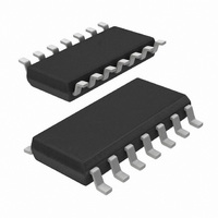
HEF4066BT,652 NXP Semiconductors, HEF4066BT,652 Datasheet - Page 3

HEF4066BT,652
Manufacturer Part Number
HEF4066BT,652
Description
IC SWITCH QUAD 1X1 14SOIC
Manufacturer
NXP Semiconductors
Series
4000Br
Specifications of HEF4066BT,652
Package / Case
14-SOIC (0.154", 3.90mm Width)
Function
Switch
Circuit
4 x 1:1
On-state Resistance
175 Ohm
Voltage Supply Source
Dual Supply
Voltage - Supply, Single/dual (±)
±3 V ~ 15 V
Current - Supply
4µA
Operating Temperature
-40°C ~ 85°C
Mounting Type
Surface Mount
Switch Configuration
SPST
On Resistance (max)
2500 Ohm @ 5 V
On Time (max)
90 ns @ 5 V
Off Time (max)
160 ns @ 5 V
Supply Voltage (max)
15.5 V
Supply Voltage (min)
4.5 V
Maximum Power Dissipation
100 mW
Maximum Operating Temperature
+ 85 C
Mounting Style
SMD/SMT
Minimum Operating Temperature
- 40 C
Propagation Delay Time
5 ns
Lead Free Status / RoHS Status
Lead free / RoHS Compliant
Lead Free Status / RoHS Status
Lead free / RoHS Compliant, Lead free / RoHS Compliant
Other names
568-1695-5
933372970652
HEF4066BTD
933372970652
HEF4066BTD
NXP Semiconductors
7. Functional description
Table 3.
[1]
8. Limiting values
Table 4.
In accordance with the Absolute Maximum Rating System (IEC 60134). Voltages are referenced to V
[1]
[2]
[3]
9. Recommended operating conditions
Table 5.
HEF4066B_6
Product data sheet
Input nE
H
L
Symbol
V
I
V
I
T
T
P
P
Symbol
V
V
T
Δt/ΔV
IK
I/O
stg
amb
amb
DD
I
tot
DD
I
H = HIGH voltage level; L = LOW voltage level.
To avoid drawing V
switch must not exceed 0.4 V. If the switch current flows into terminal nZ, no V
is no limit for the voltage drop across the switch, but the voltages at nY and nZ may not exceed V
For DIP14 packages: above T
For SO14 packages: above T
Parameter
supply voltage
input clamping current
input voltage
input/output current
storage temperature
ambient temperature
total power dissipation
power dissipation
Function table
Limiting values
Recommended operating conditions
Parameter
supply voltage
input voltage
ambient temperature
input transition rise and fall
rate
DD
current out of terminal nZ, when switch current flows into terminals nY, the voltage drop across the bidirectional
[1]
amb
amb
= 70 °C, P
= 70 °C, P
Switch
ON
OFF
All information provided in this document is subject to legal disclaimers.
tot
tot
derates linearly with 8 mW/K.
Conditions
in free air
V
V
V
derates linearly with 12 mW/K.
DD
DD
DD
= 5 V
= 10 V
= 15 V
Rev. 06 — 25 March 2010
V
T
Conditions
per switch
amb
I
DIP14
SO14
< −0.5 V or V
= −40 °C to +85 °C
I
> V
Quad single-pole single-throw analog switch
DD
DD
+ 0.5 V
current will flow out of terminals nY, in this case there
Min
3
0
−40
-
-
-
[1]
[2]
[3]
DD
Min
−0.5
-
−0.5
-
−65
−40
-
-
-
or V
Typ
-
-
-
-
-
-
SS
.
HEF4066B
SS
Max
+18
±10
V
±10
+150
+85
750
500
100
= 0 V (ground).
DD
© NXP B.V. 2010. All rights reserved.
Max
15
V
+125
3.75
0.5
0.08
DD
+ 0.5
Unit
V
mA
V
mA
°C
°C
mW
mW
mW
Unit
V
V
°C
μs/V
μs/V
μs/V
3 of 16


