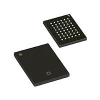
CY62146DV30LL-70BVI Cypress Semiconductor Corp, CY62146DV30LL-70BVI Datasheet

CY62146DV30LL-70BVI
Specifications of CY62146DV30LL-70BVI
Available stocks
Related parts for CY62146DV30LL-70BVI
CY62146DV30LL-70BVI Summary of contents
Page 1
... A 0 Note: 1. For best practice recommendations, please refer to the Cypress application note “System Design Guidelines” on http://www.cypress.com. Cypress Semiconductor Corporation Document #: 38-05339 Rev. *A 4-Mbit (256K x 16) Static RAM an automatic power-down feature that significantly reduces power consumption. The device can also be put into standby mode reducing power consumption by more than 99% when deselected (CE HIGH) ...
Page 2
... CY62146DV30LL CY62146DV30L 2.20V 3.0 CY62146DV30LL Notes pins are not internally connected on the die. 3. DNU pins have to be left floating or tied ensure proper application Pins H1, G2, and H6 in the BGA package are address expansion pins for 8 Mb, 16 Mb, and 32 Mb, respectively. ...
Page 3
... Output Current into Outputs (LOW)............................. 20 mA Static Discharge Voltage........................................... >2001V (per MIL-STD-883, Method 3015) Latch-up Current...................................................... >200 mA Operating Range + 0.3V CC(MAX) Device CY62146DV30L Industrial –40°C to +85°C 2.20V to 3.60V + 0.3V CC(MAX) CY62146DV30LL CY62146DV30-45 CY62146DV30-55 [5] Min. Typ. Max. Min. Typ. = 2.20V 2.0 2 ...
Page 4
Capacitance (for all packages) Parameter Description C Input Capacitance IN C Output Capacitance OUT Thermal Resistance [9] Parameter Description Θ Thermal Resistance JA (Junction to Ambient) Θ Thermal Resistance JC (Junction to Case) AC Test Loads and Waveforms R1 ...
Page 5
Switching Characteristics Over the Operating Range Parameter Description Read Cycle t Read Cycle Time RC t Address to Data Valid AA t Data Hold from Address Change OHA t CE LOW to Data Valid ACE t OE LOW to Data ...
Page 6
Switching Waveforms Read Cycle 1 (Address Transition Controlled) ADDRESS DATA OUT PREVIOUS DATA VALID [17, 18] Read Cycle No. 2 (OE Controlled) ADDRESS CE t ACE OE BHE/BLE t LZOE t DBE t LZBE HIGH IMPEDANCE DATA OUT t LZCE ...
Page 7
Switching Waveforms (continued) [15, 19, 20] Write Cycle No. 1 (WE Controlled) ADDRESS BHE/BLE OE DATA I/O NOTE 21 t HZOE [15, 19, 20] Write Cycle No. 2 (CE Controlled) ADDRESS CE WE BHE/BLE OE DATA ...
Page 8
Switching Waveforms (continued) Write Cycle No. 3 (WE Controlled, OE LOW) ADDRESS CE BHE/BLE NOTE 21 DATAI/O t Write Cycle No. 4 (BHE/BLE Controlled, OE LOW) ADDRESS CE BHE/BLE DATA I/O NOTE 21 Document ...
Page 9
... Ordering Information Speed (ns) Ordering Code 45 CY62146DV30LL-45BVI CY62146DV30LL-45BVXI CY62146DV30LL-45ZSXI 55 CY62146DV30L-55BVI CY62146DV30L-55BVXI CY62146DV30LL-55BVI CY62146DV30LL-55BVXI CY62146DV30L-55ZSXI CY62146DV30LL-55ZSXI 70 CY62146DV30L-70BVI CY62146DV30L-70BVXI CY62146DV30LL-70BVI CY62146DV30LL-70BVXI CY62146DV30L-70ZSXI CY62146DV30LL-70ZSXI Document #: 38-05339 Rev. *A Inputs/Outputs X High Z Deselect/Power-Down High Z Output Disabled L Data Out (I/O –I/O ) Read Data Out (I/O –I/O ); Read O 7 I/O – ...
Page 10
... Document #: 38-05339 Rev. *A © Cypress Semiconductor Corporation, 2005. The information contained herein is subject to change without notice. Cypress Semiconductor Corporation assumes no responsibility for the use of any circuitry other than circuitry embodied in a Cypress product. Nor does it convey or imply any license under patent or other rights. Cypress products are not warranted nor intended to be used for medical, life support, life saving, critical control or safety applications, unless pursuant to an express written agreement with Cypress ...
Page 11
Document History Page Document Title:CY62146DV30 MoBL Document Number: 38-05339 Orig. of REV. ECN NO. Issue Date Change ** 213251 See ECN *A 316039 See ECN Document #: 38-05339 Rev. *A ® 4-Mbit (256K x 16) Static RAM Description of Change ...


