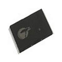
CY62167DV30LL-70ZI Cypress Semiconductor Corp, CY62167DV30LL-70ZI Datasheet - Page 3

CY62167DV30LL-70ZI
Manufacturer Part Number
CY62167DV30LL-70ZI
Description
Manufacturer
Cypress Semiconductor Corp
Datasheet
1.CY62167DV30LL-70ZI.pdf
(12 pages)
Specifications of CY62167DV30LL-70ZI
Density
16Mb
Access Time (max)
70ns
Sync/async
Asynchronous
Architecture
Not Required
Clock Freq (max)
Not RequiredMHz
Operating Supply Voltage (typ)
3V
Address Bus
20b
Package Type
TSOP-I
Operating Temp Range
-40C to 85C
Number Of Ports
1
Supply Current
25mA
Operating Supply Voltage (min)
2.2V
Operating Supply Voltage (max)
3.6V
Operating Temperature Classification
Industrial
Mounting
Surface Mount
Pin Count
48
Word Size
16b
Number Of Words
1M
Lead Free Status / Rohs Status
Not Compliant
Available stocks
Company
Part Number
Manufacturer
Quantity
Price
Company:
Part Number:
CY62167DV30LL-70ZI
Manufacturer:
CYPRESS
Quantity:
1 302
Document #: 38-05328 Rev. *F
Maximum Ratings
(Above which the useful life may be impaired. For user guide-
lines, not tested.)
Storage Temperature ................................. –65°C to +150°C
Ambient Temperature with
Power Applied............................................. –55°C to +125°C
Supply Voltage to Ground Potential .......–0.2V to V
DC Voltage Applied to Outputs
in High-Z State
DC Input Voltage
Electrical Characteristics
V
V
V
V
I
I
I
I
I
Notes:
Parameter Description
IX
OZ
CC
SB1
SB2
7. V
8. V
9. Full Device AC operation requires linear V
OH
OL
IH
IL
IL(min.)
IH(Max)
= –2.0V for pulse durations less than 20 ns.
= V
CC
Output HIGH
Voltage
Output LOW
Voltage
Input HIGH
Voltage
Input LOW
Voltage
Input
Leakage
Current
Output
Leakage
Current
V
Operating
Supply
Current
Automatic CE
Power-down
Current —
CMOS Inputs
Automatic CE
Power-down
Current —
CMOS Inputs
[7, 8]
CC
+ 0.75V for pulse durations less than 20 ns.
[7, 8]
.................................–0.2V to V
.............................–0.2V to V
I
I
I
I
V
V
V
V
GND < V
GND < V
Disabled
V
I
CMOS levels
CE
CE
V
V
f = f
Only),
V
CE
CE
V
V
f = 0, V
OH
OH
OL
OL
OUT
f = 0 (OE, WE, BHE, BLE),
IN
IN
CC
CC
CC
CC
CC
CC
IN
IN
1
2
MAX
1
2
> V
< 0.2V)
= 0.1 mA
= 2.1mA
= –0.1 mA
= –1.0 mA
> V
< 0.2V,
= 2.7V to 3.6V
= 2.7V to 3.6V
< 0.2V
= 3.60V
> V
= 2.2V to 2.7V
= 2.2V to 2.7V
= V
> V
< 0.2V,
= 0 mA
Over the Operating Range
Test Conditions
CC
(Address and Data
CC
CC
CC
CC
CCmax
CC
I
O
– 0.2V,
< V
ramp from 0 to V
< V
− 0.2V or
= 3.60V
– 0.2V or
– 0.2V or
CC
CC
, Output
V
2.20V
V
2.70V
V
2.20V
V
2.70V
f = f
1/t
f = 1 MHz
CC
CC
CC
CC
RC
MAX
CC
CC
CC
=
=
=
=
CC(min.)
+ 0.3V
+ 0.3V
+ 0.3V
L
LL
L
LL
=
> = 500 µs.
Min. Typ.
–0.3
–0.3
CY62167DV30-45
2.0
2.4
1.8
2.2
–1
–1
Output Current into Outputs (LOW)............................. 20 mA
Static Discharge Voltage.......................................... > 2001V
(per MIL-STD-883, Method 3015)
Latch-up Current..................................................... > 200 mA
Operating Range
18.5
CY62167DV30L
CY62167DV30LL
2.5
2.5
2.5
2.5
2
[6]
Device
+0.3V
+0.3V
Max. Min. Typ.
V
V
0.4
0.4
0.6
0.8
+1
+1
37
30
22
30
22
4
CC
CC
–0.3
–0.3
CY62167DV30-55
2.0
2.4
1.8
2.2
–1
–1
Industrial
Range
2.5
2.5
2.5
2.5
15
2
[6]
+0.3V
+0.3V
Max. Min. Typ.
V
V
0.4
0.4
0.6
0.8
+1
+1
30
30
22
30
22
4
CC
CC
–40°C to +85°C
Temperature
–0.3
–0.3
CY62167DV30
Ambient
CY62167DV30-70
2.0
2.4
1.8
2.2
–1
–1
2.5
2.5
2.5
2.5
12
2
[6]
MoBL
Page 3 of 12
+0.3V
+0.3V
Max.
V
V
0.4
0.4
0.6
0.8
+1
+1
25
30
22
30
22
2.20V to
4
CC
CC
V
3.60V
CC
Unit
[9]
mA
mA
®
µA
µA
µA
µA
V
V
V
V
V
V
V
V


