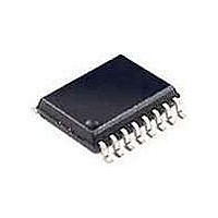
PCA9500D NXP Semiconductors, PCA9500D Datasheet - Page 9

PCA9500D
Manufacturer Part Number
PCA9500D
Description
I/O Expanders, Repeaters & Hubs I/O EXPANDER W/2K EE
Manufacturer
NXP Semiconductors
Datasheet
1.PCA9500PW112.pdf
(26 pages)
Specifications of PCA9500D
Logic Family
PCA
Number Of Lines (input / Output)
8 / 8
Operating Supply Voltage
2.5 V to 3.6 V
Operating Temperature Range
- 40 C to + 85 C
Package / Case
SOT-109
Mounting Style
SMD/SMT
Number Of Input Lines
8
Number Of Output Lines
8
Lead Free Status / Rohs Status
Details
Other names
PCA9500D,112
Available stocks
Company
Part Number
Manufacturer
Quantity
Price
Company:
Part Number:
PCA9500D
Manufacturer:
SHRP
Quantity:
3 116
Part Number:
PCA9500D
Manufacturer:
PHILIPS/飞利浦
Quantity:
20 000
NXP Semiconductors
PCA9500_4
Product data sheet
Fig 13. Random read
Fig 14. Sequential read
SDA
SDA
S
START condition
1
S
START condition
slave address (memory)
7.4.2.2 Random read
7.4.2.3 Sequential read
0
1
slave address (memory)
1
0
0 A2 A1 A0
1
The PCA9500's random read mode allows the address to be read from to be specified by
the master. This is done by performing a dummy write to set the address counter to the
location to be read. The master must perform a byte write to the address location to be
read, but instead of transmitting the data after receiving the acknowledge from the
PCA9500, the master re-issues the START condition and memory slave address with the
R/W bit set to one. The PCA9500 will then transmit an acknowledge and use the next
eight clock cycles to transmit the data contained in the addressed location. The master
ceases the transmission by issuing the STOP condition after the eighth bit, omitting the
ninth clock cycle acknowledge.
The PCA9500 sequential read is an extension of either the current address read or
random read. If the master does not issue a STOP condition after it has received the
eighth data bit, but instead issues an acknowledge, the PCA9500 will increment the
address counter and use the next eight cycles to transmit the data from that location. The
master can continue this process to read the contents of the entire memory. Upon
reaching address 255 the counter will return to address 0 and continue transmitting data
until a STOP condition is received. The master ceases the transmission by issuing the
STOP condition after the eighth bit, omitting the ninth clock cycle acknowledge.
Fig 12. Current address read
0 A2 A1 A0
R/W
0
SDA
R/W
A
acknowledge
from slave
1
S
START condition
A
acknowledge
from slave
1
word address
slave address (memory)
data from memory
0
Rev. 04 — 15 April 2009
DATA n
1
acknowledge
from slave
0 A2 A1 A0
acknowledge
from master
8-bit I
A
S
START condition
A
R/W
2
1
1
C-bus and SMBus I/O port with 2-kbit EEPROM
slave address (memory)
data from memory
A
acknowledge
from slave
0
DATA n + 1
1
0 A2 A1 A0
acknowledge
data from memory
from master
acknowledge
from slave
A
R/W
1
A
data from memory
DATA n + X
data from memory
P
STOP condition
PCA9500
© NXP B.V. 2009. All rights reserved.
002aae596
condition
002aae598
STOP
condition
002aae597
STOP
P
P
9 of 26


