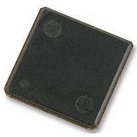
H5PS1G63EFR-S6C HYNIX SEMICONDUCTOR, H5PS1G63EFR-S6C Datasheet - Page 41

H5PS1G63EFR-S6C
Manufacturer Part Number
H5PS1G63EFR-S6C
Description
58T1894
Manufacturer
HYNIX SEMICONDUCTOR
Datasheet
1.H5PS1G63EFR-S6C.pdf
(44 pages)
Specifications of H5PS1G63EFR-S6C
Memory Type
SDRAM
Memory Configuration
64M X 16
Access Time
15ns
Memory Case Style
FBGA
No. Of Pins
84
Operating Temperature Range
0°C To +85°C
Memory Size
1 Gbit
Rohs Compliant
Yes
Available stocks
Company
Part Number
Manufacturer
Quantity
Price
Company:
Part Number:
H5PS1G63EFR-S6C
Manufacturer:
HYNIX
Quantity:
9 500
Company:
Part Number:
H5PS1G63EFR-S6C
Manufacturer:
PEAK
Quantity:
3 000
Company:
Part Number:
H5PS1G63EFR-S6C
Manufacturer:
FBGA
Quantity:
4 800
Part Number:
H5PS1G63EFR-S6C
Manufacturer:
HYNIX/海力士
Quantity:
20 000
Company:
Part Number:
H5PS1G63EFR-S6C-
Manufacturer:
HYNIX
Quantity:
2 526
Company:
Part Number:
H5PS1G63EFR-S6C-C
Manufacturer:
VIA
Quantity:
1 000
Rev. 0.4 / Nov 2008
272 ps = + 672 ps. Similarly, tLZ (DQ) for DDR2-667 derates to tLZ (DQ), min (derated) = - 900 ps - 293
ps = - 1193 ps and tLZ (DQ), max (derated) = 450 ps + 272 ps = + 722 ps. (Caution on the min/max
usage!)
41. When the device is operated with input clock jitter, this parameter needs to be derated by the actual
tJIT (per) of the input clock. (output deratings are relative to the SDRAM input clock.)
For example, if the measured jitter into a DDR2-667 SDRAM has tJIT (per), min = - 72 ps and tJIT (per),
max = + 93 ps, then tRPRE, min (derated) = tRPRE, min + tJIT (per), min = 0.9 x tCK (avg) - 72 ps = +
2178 ps and tRPRE, max (derated) = tRPRE, max + tJIT (per), max = 1.1 x tCK (avg) + 93 ps = + 2843
ps. (Caution on the min/max usage!)
42. When the device is operated with input clock jitter, this parameter needs to be derated by the actual
tJIT (duty) of the input clock. (output deratings are relative to the SDRAM input clock.)
For example, if the measured jitter into a DDR2-667 SDRAM has tJIT (duty), min = - 72 ps and tJIT (duty),
max = + 93 ps, then tRPST, min (derated) = tRPST, min + tJIT (duty), min = 0.4 x tCK (avg) - 72 ps = +
928 ps and tRPST, max (derated) = tRPST, max + tJIT (duty), max = 0.6 x tCK (avg) + 93 ps = + 1592 ps.
(Caution on the min/max usage!)
43. When the device is operated with input clock jitter, this parameter needs to be derated by {-
tJIT (duty), max - tERR(6-10per),max} and {- tJIT (duty), min - tERR(6-10per),min} of the actual input
clock.(output deratings are relative to the SDRAM input clock.)
For example, if the measured jitter into a DDR2-667 SDRAM has tERR(6-10per),min = - 272 ps, tERR(6-
10per), max = + 293 ps, tJIT (duty), min = - 106 ps and tJIT (duty), max = + 94 ps, then tAOF, min (der-
ated) = tAOF, min + {- tJIT (duty), max - tERR(6-10per),max} = - 450 ps + {- 94 ps - 293 ps} = - 837 ps
and tAOF, max (derated) = tAOF, max + {- tJIT (duty), min - tERR(6-10per),min} = 1050 ps + {106 ps +
272 ps} = + 1428 ps. (Caution on the min/max usage!)
44. For tAOFD of DDR2-400/533, the 1/2 clock of tCK in the 2.5 x tCK assumes a tCH, input clock HIGH
pulse width of 0.5 relative to tCK. tAOF, min and tAOF, max should each be derated by the same amount
as the actual amount of tCH offset present at the DRAM input with respect to 0.5. For example, if an input
clock has a worst case tCH of 0.45, the tAOF, min should be derated by subtracting 0.05 x tCK from it,
whereas if an input clock has a worst case tCH of 0.55, the tAOF, max should be derated by adding 0.05 x
tCK to it. Therefore, we have;
tAOF, min (derated) = tAC, min - [0.5 - Min(0.5, tCH, min)] x tCK
tAOF, max (derated) = tAC, max + 0.6 + [Max(0.5, tCH, max) - 0.5] x tCK
or
tAOF, min (derated) = Min (tAC, min, tAC, min - [0.5 - tCH, min] x tCK)
tAOF, max (derated) = 0.6 + Max (tAC, max, tAC, max + [tCH, max - 0.5] x tCK)
where tCH, min and tCH, max are the minimum and maximum of tCH actually measured at the DRAM
input balls.
45. For tAOFD of DDR2-667/800, the 1/2 clock of nCK in the 2.5 x nCK assumes a tCH (avg), average input
clock HIGH pulse width of 0.5 relative to tCK (avg). tAOF, min and tAOF, max should each be derated by
the same amount as the actual amount of tCH (avg) offset present at the DRAM input with respect to 0.5.
For example, if an input clock has a worst case tCH (avg) of 0.48, the tAOF, min should be derated by sub-
H5PS1G43EFR
H5PS1G83EFR
H5PS1G63EFR
41


