STM32F407IGT6 STMicroelectronics, STM32F407IGT6 Datasheet - Page 7
STM32F407IGT6
Manufacturer Part Number
STM32F407IGT6
Description
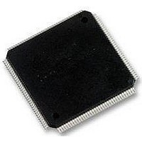
IC MCU 32BIT 1MB FLASH 176LQFP
Manufacturer
STMicroelectronics
Specifications of STM32F407IGT6
Core Processor
ARM Cortex-M4
Core Size
32-Bit
Speed
168MHz
Connectivity
CAN, I²C, IrDA, LIN, SPI, UART/USART, USB OTG
Peripherals
Brown-out Detect/Reset, DMA, I²S, POR, PWM, WDT
Number Of I /o
140
Program Memory Size
1MB (1M x 8)
Program Memory Type
FLASH
Eeprom Size
-
Ram Size
192K x 8
Voltage - Supply (vcc/vdd)
1.8 V ~ 3.6 V
Data Converters
A/D 24x12b; D/A 2x12b
Oscillator Type
Internal
Operating Temperature
-40°C ~ 85°C
Package / Case
*
Core
ARM Cortex M4
Processor Series
STM32F4
Data Bus Width
32 bit
Maximum Clock Frequency
168 MHz
Data Ram Size
192 KB
On-chip Adc
Yes
Number Of Programmable I/os
140
Number Of Timers
10
Operating Supply Voltage
1.7 V to 3.6 V
Mounting Style
SMD/SMT
A/d Bit Size
12 bit
A/d Channels Available
24
Interface Type
CAN, I2C, I2S, SPI, UART
Lead Free Status / Rohs Status
Lead free / RoHS Compliant
Other names
497-11604
Available stocks
Company
Part Number
Manufacturer
Quantity
Price
Company:

Part Number:
STM32F407IGT6
Manufacturer:
ST
Quantity:
10 000
Company:
Part Number:
STM32F407IGT6
Manufacturer:
STMicroelectronics
Quantity:
10 000
Part Number:
STM32F407IGT6
Manufacturer:
ST
Quantity:
20 000
Company:
Part Number:
STM32F407IGT6.
Manufacturer:
EXAR
Quantity:
15 225


STM32F405xx, STM32F407xx
List of figures
Figure 1.
Figure 2.
Figure 3.
Figure 4.
Figure 5.
Figure 6.
Figure 7.
Figure 8.
Figure 9.
Figure 10.
Figure 11.
Figure 12.
Figure 13.
Figure 14.
Figure 15.
Figure 16.
Figure 17.
Figure 18.
Figure 19.
Figure 20.
Figure 21.
Figure 22.
Figure 23.
Figure 24.
Figure 25.
Figure 26.
Figure 27.
Figure 28.
Figure 29.
Figure 30.
Figure 31.
Figure 32.
Figure 33.
Figure 34.
Figure 35.
Figure 36.
Figure 37.
Figure 38.
Figure 39.
Figure 40.
Figure 41.
Figure 42.
Figure 43.
Figure 44.
Compatible board design between STM32F2xx and STM32F4xx: LQFP176 . . . . . . . . . . 13
Compatible board design between STM32F1xx/STM32F2xx/ . . . . . . . . . . . . . . . . . . . . . . . .
STM32F4xx: LQFP144 . . . . . . . . . . . . . . . . . . . . . . . . . . . . . . . . . . . . . . . . . . . . . . . . . . . . 14
Compatible board design STM32F1xx/STM32F2xx/
STM32F4xx: LQFP100 . . . . . . . . . . . . . . . . . . . . . . . . . . . . . . . . . . . . . . . . . . . . . . . . . . . . 14
Compatible board design between STM32F1xx/STM32F4xx: LQFP64 . . . . . . . . . . . . . . . 15
STM32F40x block diagram . . . . . . . . . . . . . . . . . . . . . . . . . . . . . . . . . . . . . . . . . . . . . . . . . 16
Multi-AHB matrix . . . . . . . . . . . . . . . . . . . . . . . . . . . . . . . . . . . . . . . . . . . . . . . . . . . . . . . . . 19
Regulator ON/internal reset OFF . . . . . . . . . . . . . . . . . . . . . . . . . . . . . . . . . . . . . . . . . . . . 23
Startup in regulator OFF: slow V
- power-down reset risen after V
Startup in regulator OFF mode: fast V
- power-down reset risen before V
STM32F40x LQFP64 pinout . . . . . . . . . . . . . . . . . . . . . . . . . . . . . . . . . . . . . . . . . . . . . . . . 38
STM32F40x LQFP100 pinout . . . . . . . . . . . . . . . . . . . . . . . . . . . . . . . . . . . . . . . . . . . . . . . 39
STM32F40x LQFP144 pinout . . . . . . . . . . . . . . . . . . . . . . . . . . . . . . . . . . . . . . . . . . . . . . . 40
STM32F40x LQFP176 pinout . . . . . . . . . . . . . . . . . . . . . . . . . . . . . . . . . . . . . . . . . . . . . . . 41
STM32F40x UFBGA176 ballout . . . . . . . . . . . . . . . . . . . . . . . . . . . . . . . . . . . . . . . . . . . . . 42
Memory map . . . . . . . . . . . . . . . . . . . . . . . . . . . . . . . . . . . . . . . . . . . . . . . . . . . . . . . . . . . . 54
Pin loading conditions . . . . . . . . . . . . . . . . . . . . . . . . . . . . . . . . . . . . . . . . . . . . . . . . . . . . . 55
Pin input voltage . . . . . . . . . . . . . . . . . . . . . . . . . . . . . . . . . . . . . . . . . . . . . . . . . . . . . . . . . 55
Power supply scheme . . . . . . . . . . . . . . . . . . . . . . . . . . . . . . . . . . . . . . . . . . . . . . . . . . . . 56
Current consumption measurement scheme . . . . . . . . . . . . . . . . . . . . . . . . . . . . . . . . . . . 57
External capacitor C
High-speed external clock source AC timing diagram . . . . . . . . . . . . . . . . . . . . . . . . . . . . 74
Low-speed external clock source AC timing diagram . . . . . . . . . . . . . . . . . . . . . . . . . . . . . 74
Typical application with an 8 MHz crystal . . . . . . . . . . . . . . . . . . . . . . . . . . . . . . . . . . . . . . 75
Typical application with a 32.768 kHz crystal . . . . . . . . . . . . . . . . . . . . . . . . . . . . . . . . . . . 76
ACC
PLL output clock waveforms in center spread mode . . . . . . . . . . . . . . . . . . . . . . . . . . . . . 82
PLL output clock waveforms in down spread mode . . . . . . . . . . . . . . . . . . . . . . . . . . . . . . 82
I/O AC characteristics definition . . . . . . . . . . . . . . . . . . . . . . . . . . . . . . . . . . . . . . . . . . . . . 91
Recommended NRST pin protection . . . . . . . . . . . . . . . . . . . . . . . . . . . . . . . . . . . . . . . . . 92
I
SPI timing diagram - slave mode and CPHA = 0 . . . . . . . . . . . . . . . . . . . . . . . . . . . . . . . . 98
SPI timing diagram - slave mode and CPHA = 1
SPI timing diagram - master mode
I
I
USB OTG FS timings: definition of data signal rise and fall time . . . . . . . . . . . . . . . . . . . 103
ULPI timing diagram . . . . . . . . . . . . . . . . . . . . . . . . . . . . . . . . . . . . . . . . . . . . . . . . . . . . . 104
Ethernet SMI timing diagram . . . . . . . . . . . . . . . . . . . . . . . . . . . . . . . . . . . . . . . . . . . . . . 105
Ethernet RMII timing diagram . . . . . . . . . . . . . . . . . . . . . . . . . . . . . . . . . . . . . . . . . . . . . . 106
Ethernet MII timing diagram . . . . . . . . . . . . . . . . . . . . . . . . . . . . . . . . . . . . . . . . . . . . . . . 106
ADC accuracy characteristics . . . . . . . . . . . . . . . . . . . . . . . . . . . . . . . . . . . . . . . . . . . . . . 110
Typical connection diagram using the ADC . . . . . . . . . . . . . . . . . . . . . . . . . . . . . . . . . . . 110
Power supply and reference decoupling (V
Power supply and reference decoupling (V
2
2
2
C bus AC waveforms and measurement circuit . . . . . . . . . . . . . . . . . . . . . . . . . . . . . . . . 96
S slave timing diagram (Philips protocol)
S master timing diagram (Philips protocol)
LSI
versus temperature . . . . . . . . . . . . . . . . . . . . . . . . . . . . . . . . . . . . . . . . . . . . . . . . 78
EXT
. . . . . . . . . . . . . . . . . . . . . . . . . . . . . . . . . . . . . . . . . . . . . . . . . . . 61
Doc ID 022152 Rev 1
CAP_1
DD
CAP_1
(1)
slope
. . . . . . . . . . . . . . . . . . . . . . . . . . . . . . . . . . . . . . . . . 99
DD
/V
/V
CAP_2
slope
CAP_2
(1)
REF+
REF+
(1)
. . . . . . . . . . . . . . . . . . . . . . . . . . . . . . . . . . 101
. . . . . . . . . . . . . . . . . . . . . . . . . . . . . . . . . 101
stabilization . . . . . . . . . . . . . . . . . . . . . . . . 25
(1)
not connected to V
connected to V
stabilization . . . . . . . . . . . . . . . . . . . . . . 25
. . . . . . . . . . . . . . . . . . . . . . . . . . . . . . 98
DDA
DDA
). . . . . . . . . . . . . . . . 111
). . . . . . . . . . . . . 111
List of figures
7/154
Related parts for STM32F407IGT6
Image
Part Number
Description
Manufacturer
Datasheet
Request
R

Part Number:
Description:
Microsoft .NET Micro Framework environment for STM32F4 microcontrollers
Manufacturer:
STMICROELECTRONICS [STMicroelectronics]
Datasheet:

Part Number:
Description:
DEV KIT FOR STM32
Manufacturer:
STMicroelectronics
Datasheet:

Part Number:
Description:
MCU ARM 128KB FLASH MEM 64-LQFP
Manufacturer:
STMicroelectronics
Datasheet:

Part Number:
Description:
MCU ARM 32BIT 128KB FLASH 64BGA
Manufacturer:
STMicroelectronics
Datasheet:

Part Number:
Description:
MCU ARM 32BIT 256K FLASH 144LQFP
Manufacturer:
STMicroelectronics
Datasheet:

Part Number:
Description:
KIT STARTER FOR STM32F10X
Manufacturer:
STMicroelectronics
Datasheet:

Part Number:
Description:
MCU ARM 128K FLASH/TIMER
Manufacturer:
STMicroelectronics
Datasheet:

Part Number:
Description:
MCU ARM 128KB FLASH MEM 100-LQFP
Manufacturer:
STMicroelectronics
Datasheet:

Part Number:
Description:
MCU 32BIT ARM 64K FLASH 36VFQFPN
Manufacturer:
STMicroelectronics
Datasheet:
Part Number:
Description:
MCU ARM 32BIT 32KB FLASH 48LQFP
Manufacturer:
STMicroelectronics
Datasheet:
Part Number:
Description:
MCU ARM 32BIT 64KB FLASH 64LQFP
Manufacturer:
STMicroelectronics
Datasheet:
Part Number:
Description:
MCU ARM 32BIT 384KB FLASH 64LQFP
Manufacturer:
STMicroelectronics
Datasheet:

Part Number:
Description:
MCU 32BIT ARM 512K FLASH 100-LQF
Manufacturer:
STMicroelectronics
Datasheet:
Part Number:
Description:
MCU ARM 32BIT 512KB FLASH 144BGA
Manufacturer:
STMicroelectronics
Datasheet:
Part Number:
Description:
MCU ARM 32BIT 512K FLASH 144LQFP
Manufacturer:
STMicroelectronics
Datasheet: