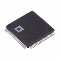
AD8110AST Analog Devices Inc, AD8110AST Datasheet - Page 17

AD8110AST
Manufacturer Part Number
AD8110AST
Description
IC VIDEO CROSSPOINT SWIT 80LQFP
Manufacturer
Analog Devices Inc
Datasheet
1.AD8111ASTZ.pdf
(28 pages)
Specifications of AD8110AST
Rohs Status
RoHS non-compliant
Function
Video Crosspoint Switch
Circuit
1 x 16:8
Voltage Supply Source
Dual Supply
Voltage - Supply, Single/dual (±)
±4.5 V ~ 5.5 V
Operating Temperature
-40°C ~ 85°C
Mounting Type
Surface Mount
Package / Case
80-LQFP
Array Configuration
16x8
Number Of Arrays
1
Screening Level
Industrial
Pin Count
80
Package Type
LQFP
Power Supply Requirement
Dual
Lead Free Status / RoHS Status
Not Compliant
Available stocks
Company
Part Number
Manufacturer
Quantity
Price
Company:
Part Number:
AD8110AST
Manufacturer:
Analog Devices Inc.
Quantity:
2
Company:
Part Number:
AD8110AST
Manufacturer:
ADI
Quantity:
846
Part Number:
AD8110AST
Manufacturer:
ADI/亚德诺
Quantity:
20 000
Company:
Part Number:
AD8110ASTZ
Manufacturer:
ADI
Quantity:
160
Company:
Part Number:
AD8110ASTZ
Manufacturer:
Analog Devices Inc
Quantity:
10 000
Part Number:
AD8110ASTZ
Manufacturer:
ADI/亚德诺
Quantity:
20 000
The basic concept in constructing larger crosspoint arrays is to
connect inputs in parallel in a horizontal direction and to
“wire-OR” the outputs together in the vertical direction. The
meaning of horizontal and vertical can best be understood by
looking at a diagram. Figure 6 illustrates this concept for a 32 × 8
crosspoint array.
The inputs are each uniquely assigned to each of the 32 inputs
of the two devices and terminated appropriately. The outputs
are wire-ORed together in pairs. The output from only one of a
wired OR pair should be enabled at any given time. The device
programming software must be properly written to cause this
to happen.
IN 00–15
IN 16–31
×
IN 00–15
IN 16–31
IN 32–47
IN 48–63
IN 64–79
IN 80–95
IN 96–111
IN 112–127
R
R
TERM
TERM
16
16
16
16
16
16
16
16
16
16
16
16
R
R
R
R
R
R
R
R
TERM
TERM
TERM
TERM
TERM
TERM
TERM
TERM
AD8110
AD8111
AD8110
AD8111
OR
OR
8
8
(8 x AD8110)
AD8110
AD8110
AD8110
AD8110
AD8110
AD8110
AD8110
AD8110
RANK 1
128:16
4
4
4
4
4
4
4
4
4
4
4
4
4
4
4
4
×
4
1k
4
1k
4
1k
4
1k
At some point, the number of outputs that are wire-ORed becomes
too great to maintain system performance. This will vary according
to which system specifications are most important. It will also depend
on whether the matrix consists of AD8110s or AD8111s. The
output disabled impedance of the AD8110 is much higher than
that of the AD8111, so its disabled parasitics will have a smaller
effect on the one output that is enabled. For example, a 128 × 8
crosspoint can be created with eight AD8110/AD8111s. This
design will have 128 separate inputs and have the corresponding
outputs of each device wire-ORed together in groups of eight.
Using additional crosspoint devices in the design can lower the
number of outputs that must be wire-ORed together. Figure 7
shows a block diagram of a system using eight AD8110s and
two AD8111s to create a nonblocking, gain-of-two, 128 × 8
crosspoint that restricts the wire-ORing at the output to only
four outputs. These devices are the AD8110, which has a higher
disabled output impedance than the AD8111.
Additionally, by using the lower four outputs from each of the
two Rank 2 AD8111s, a blocking 128 × 16 crosspoint array can
be realized. There are, however, some drawbacks to this tech-
nique. The offset voltages of the various cascaded devices will
accumulate and the bandwidth limitations of the devices will
compound. In addition, the extra devices will consume more
current and take up more board space. Once again, the overall
system design specifications will determine how to make the
various tradeoffs.
16:8 NONBLOCKING
(16:16 BLOCKING)
AD8111
AD8111
RANK 2
4
4
4
4
×
OUT 00 – 07
NONBLOCKING
ADDITIONAL
8 OUTPUTS
(SUBJECT
TO BLOCKING)
AD8110/AD8111


