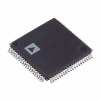
AD8110AST Analog Devices Inc, AD8110AST Datasheet - Page 20

AD8110AST
Manufacturer Part Number
AD8110AST
Description
IC VIDEO CROSSPOINT SWIT 80LQFP
Manufacturer
Analog Devices Inc
Datasheet
1.AD8111ASTZ.pdf
(28 pages)
Specifications of AD8110AST
Rohs Status
RoHS non-compliant
Function
Video Crosspoint Switch
Circuit
1 x 16:8
Voltage Supply Source
Dual Supply
Voltage - Supply, Single/dual (±)
±4.5 V ~ 5.5 V
Operating Temperature
-40°C ~ 85°C
Mounting Type
Surface Mount
Package / Case
80-LQFP
Array Configuration
16x8
Number Of Arrays
1
Screening Level
Industrial
Pin Count
80
Package Type
LQFP
Power Supply Requirement
Dual
Lead Free Status / RoHS Status
Not Compliant
Available stocks
Company
Part Number
Manufacturer
Quantity
Price
Company:
Part Number:
AD8110AST
Manufacturer:
Analog Devices Inc.
Quantity:
2
Company:
Part Number:
AD8110AST
Manufacturer:
ADI
Quantity:
846
Part Number:
AD8110AST
Manufacturer:
ADI/亚德诺
Quantity:
20 000
Company:
Part Number:
AD8110ASTZ
Manufacturer:
ADI
Quantity:
160
Company:
Part Number:
AD8110ASTZ
Manufacturer:
Analog Devices Inc
Quantity:
10 000
Part Number:
AD8110ASTZ
Manufacturer:
ADI/亚德诺
Quantity:
20 000
AD8110/AD8111
From a circuit standpoint, this output crosstalk mechanism
looks like a transformer with a mutual inductance between the
windings that drives a load resistor. For low frequencies, the
magnitude of the crosstalk is given by:
where Mxy is the mutual inductance of output x to output y,
and R
crosstalk mechanism can be minimized by keeping the mutual
inductance low and increasing R
be kept low by increasing the spacing of the conductors and
minimizing their parallel length.
PCB Layout
Extreme care must be exercised to minimize additional crosstalk
generated by the system circuit board(s). The areas that must be
carefully detailed are grounding, shielding, signal routing, and
supply bypassing.
The packaging of the AD8110/AD8111 is designed to help keep
the crosstalk to a minimum. Each input is separated from each
other input by an analog ground pin. All of these AGNDs should
be directly connected to the ground plane of the circuit board.
These ground pins provide shielding, low impedance return
paths and physical separation for the inputs. All of these help to
reduce crosstalk.
Each output is separated from its two neighboring outputs by an
analog ground pin in addition to an analog supply pin of one
polarity or the other. Each of these analog supply pins provides
power to the output stages of only the two nearest outputs. These
supply pins and analog grounds provide shielding, physical
separation and a low impedance supply for the outputs. Individual
bypassing of each of these supply pins with a 0.01 µF chip capaci-
tor directly to the ground plane minimizes high frequency output
crosstalk via the mechanism of sharing common impedances.
Each output also has an on-chip compensation capacitor that is
individually tied to the nearby analog ground pins AGND00
through AGND07. This technique reduces crosstalk by prevent-
ing the currents that flow in these paths from sharing a common
impedance on the IC and in the package pins. These AGNDxx
signals should all be directly connected to the ground plane.
The input and output signals will have minimum crosstalk if
they are located between ground planes on layers above and
below, and separated by ground in between. Vias should be
located as close to the IC as possible to carry the inputs and
outputs to the inner layer. The only place the input and output
signals surface is at the input termination resistors and the out-
put series back termination resistors. These signals should also
be separated, to the extent possible, as soon as they emerge from
the IC package.
Windows is a registered trademark of Microsoft Corporation
L
is the load resistance on the measured output. This
XT
=
20
log
10
L
(
. The mutual inductance can
Mxy s R
×
/
L
)
Evaluation Board
A four-layer evaluation board is available for the AD8110/AD8111.
The exact same board and external components are used for
each device. The only difference is the device itself, which offers
a selection of a gain of unity or gain of two through the analog
channels. This board has been carefully laid out and tested to
demonstrate the specified high-speed performance of the device.
Figure 9 shows the schematic of the evaluation board. Figure 10
shows the component side silk-screen. The layouts of the board’s
four layers are given in:
Component Layer—Figure 11
Signal Routing Layer—Figure 12
Power Layer—Figure 13
Bottom Layer—Figure 14
The evaluation board package includes the following:
•
•
•
•
Optimized for video applications, all signal inputs and outputs
are terminated with 75 Ω resistors. Stripline techniques are used
to achieve a characteristic impedance on the signal input and
output lines also of 75 Ω. Figure 8 shows a cross-section of one
of the input or output tracks along with the arrangement of the
PCB layers. It should be noted that unused regions of the four
layers are filled up with ground planes. As a result, the input
and output traces, in addition to having controlled impedances,
are well shielded.
The board has 24 BNC type connectors: 16 inputs and 8 outputs.
The connectors are arranged in a crescent around the device. As
can be seen from Figure 12, this results in all 16 input signal
traces and all eight signal output traces having the same length.
This is useful in tests such as All-Hostile Crosstalk where the
phase relationship and delay between signals needs to be
maintained from input to output.
Fully populated board with BNC-type connectors.
Windows
via the printer port.
Custom cable to connect evaluation board to PC.
Disk containing Gerber files of board layout.
b = 0.024"
(0.6mm)
®
based software for controlling the board from a PC
a = 0.008"
(0.2mm)
w = 0.008"
(0.2mm)
h = 0.011325"
(0.288mm)
t = 0.00135" (0.0343mm)
TOP LAYER
SIGNAL LAYER
POWER LAYER
BOTTOM LAYER


