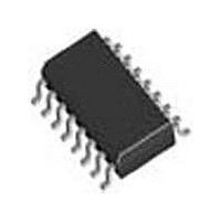
SI3018-F-GSR Silicon Laboratories Inc, SI3018-F-GSR Datasheet - Page 46

SI3018-F-GSR
Manufacturer Part Number
SI3018-F-GSR
Description
Manufacturer
Silicon Laboratories Inc
Datasheet
1.SI3018-F-GSR.pdf
(111 pages)
Specifications of SI3018-F-GSR
Lead Free Status / Rohs Status
Supplier Unconfirmed
- Current page: 46 of 111
- Download datasheet (2Mb)
In Figure 35 the CID field is 0. As this field is decremented in LSB to MSB order, the value decrements for each SDI
down the line. The BRCT and R/W bits remain unchanged as the control word passes through the entire chain. A
unique CID is presented to each device, and the device receiving a CID value of 0 is the target of the operation
(channel 0 in this case). Figure 36 illustrates that in broadcast mode, all bits pass through the chain without
permutation.
Figure 37 and Figure 38 illustrate WRITE and READ operations via an 8-bit SPI controller. Each of these
operations are performed as a 3-byte transfer. The CS pin is asserted between each byte. The CS pin must be
asserted before the first falling edge of SCLK after the DATA byte to indicate to the state machine that only one
byte should be transferred. The state of the SDI pin is ignored during the DATA byte of a read operation.
CS B
S CLK
S DI
S DO
SDI0-15
CS B
S CLK
S DI
S DO
CSB
SCLK
SDI
SDO
Figure 36. Sample SPI Control Byte for Broadcast Mode (Write Only)
CONTROL
CONTROL
1
CONTROL
Figure 37. Write Operation via an 8-bit SPI Port
Figure 38. Read Operation via an 8-bit SPI Port
Figure 39. Write Operation via a 16-bit SPI Port
0
A DDRE S S
1
A DDRE S S
Rev. 1.31
ADDRESS
0
Data [7:0]
X
Si3050 + Si3018/19
DA TA [7:0]
XXXXXXXXXXXX
X
X X X X X X X X
Data [7:0]
X
Hi-Z
X
Hi - Z
47
Related parts for SI3018-F-GSR
Image
Part Number
Description
Manufacturer
Datasheet
Request
R
Part Number:
Description:
TSSOP 16/C�/SI3050 GLOBAL VOICE DAA LINE-SIDE - LEAD-FREE
Manufacturer:
Silicon Laboratories Inc
Part Number:
Description:
IC VOICE DAA GCI/PCM/SPI 16TSSOP
Manufacturer:
Silicon Laboratories Inc
Datasheet:

Part Number:
Description:
IC VOICE DAA GCI/PCM/SPI 16SOIC
Manufacturer:
Silicon Laboratories Inc
Datasheet:

Part Number:
Description:
IC VOICE DAA GCI/PCM/SPI 16SOIC
Manufacturer:
Silicon Laboratories Inc
Datasheet:

Part Number:
Description:
Modem Chip Chipset 16-Pin SOIC T/R
Manufacturer:
Silicon Laboratories Inc
Datasheet:
Part Number:
Description:
IC VOICE DAA GCI/PCM/SPI 16SOIC
Manufacturer:
Silicon Laboratories Inc

Part Number:
Description:
IC VOICE DAA GCI/PCM/SPI 16SOIC
Manufacturer:
Silicon Laboratories Inc
Datasheet:

Part Number:
Description:
IC VOICE DAA GCI/PCM/SPI 16SOIC
Manufacturer:
Silicon Laboratories Inc
Datasheet:

Part Number:
Description:
IC VOICE DAA GCI/PCM/SPI 16SOIC
Manufacturer:
Silicon Laboratories Inc
Datasheet:
Part Number:
Description:
IC VOICE DAA GCI/PCM/SPI 16TSSOP
Manufacturer:
Silicon Laboratories Inc
Datasheet:
Part Number:
Description:
IC VOICE DAA GCI/PCM/SPI 16TSSOP
Manufacturer:
Silicon Laboratories Inc
Part Number:
Description:
SMD/C�/SINGLE-ENDED OUTPUT SILICON OSCILLATOR
Manufacturer:
Silicon Laboratories Inc
Part Number:
Description:
Manufacturer:
Silicon Laboratories Inc
Datasheet:
Part Number:
Description:
N/A N/A/SI4010 AES KEYFOB DEMO WITH LCD RX
Manufacturer:
Silicon Laboratories Inc
Datasheet:


